 Skip to content
Getting component spacing wrong is a headache you don't need. It can lead to shorts, open circuits, or a board that's impossible to rework. The pressure to shrink designs often tempts us to place parts closer than we should.
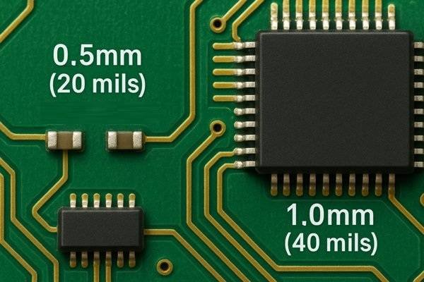
The minimum component spacing for reflow soldering depends on the component type, with a general guideline of 0.5mm (20 mils) between smaller passive components like 0402 resistors and 1.0mm (40 mils) around larger ICs. These values are baseline recommendations and should be verified against your assembly house's specific capabilities.
I've learned this lesson the hard way. Early in my career, I pushed components so close together on a dense security keypad project that our yields plummeted. It was a costly mistake in both time and money. Understanding and respecting these spacing rules is fundamental to designing a product that can be manufactured reliably. Let's dig into the details.
What Are The IPC Standards For Component Clearance In PCB Assembly?
Are you confused by which IPC standard to follow for component spacing? With multiple documents out there, it's easy to get lost. You need clear, authoritative guidance to ensure your design is manufacturable and reliable.
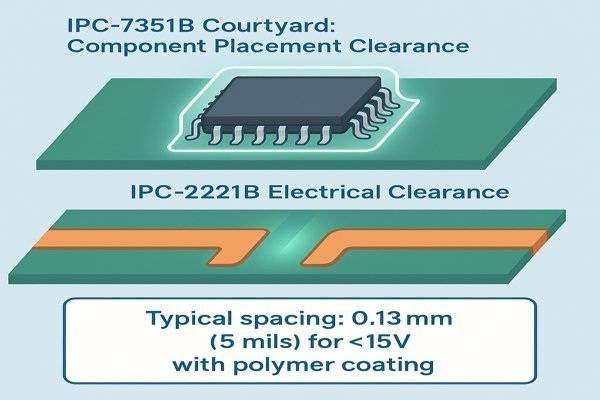
The primary standard is IPC-7351B, which focuses on land pattern design and component "courtyards." For electrical clearance between conductors, IPC-2221B is the key reference. A minimum spacing of 0.13mm (5 mils) is often cited for general-purpose external conductors with a permanent polymer coating under 15V.
Understanding the Key IPC Design Standards
When I first started designing boards, I thought of IPC standards as just a set of rigid rules. But over the years, I've come to see them as a shared language between me and the manufacturer. They prevent misunderstandings that lead to costly errors. Let's break down the two most important standards for component spacing.
IPC-7351B1: The Land Pattern Standard for Assembly
This standard defines a "courtyard" around each component's land pattern. This courtyard is a keep-out area that accounts for manufacturing tolerances and ensures enough space for placement, soldering, and rework. The standard defines three density levels, which represent a trade-off between board size and ease of manufacturing.
- Level A (Maximum): Best for low-density, high-reliability products like industrial or aerospace systems. The larger spacing makes the board easier to manufacture and, crucially, easier to repair in the field.
- Level B (Nominal): This is the most common middle ground. It provides a good balance between density and manufacturability. I use this as the default for most of my projects.
- Level C (Minimum): Used for extremely dense, miniaturized products like wearables or mobile devices where space is the absolute priority. This level assumes rework is less likely or will be done with specialized, high-precision equipment.
The table below summarizes these levels:
| Density Level | Name | Typical Use Case | Approx. Courtyard Excess |
|---|---|---|---|
| Level A | Maximum | Low-density, high-reliability (e.g., industrial) | ~0.50 mm |
| Level B | Nominal | Moderate density, good balance (most products) | ~0.25 mm |
| Level C | Minimum | High-density, miniaturized (e.g., wearables) | ~0.10 mm |
IPC-2221B2: The Standard for Electrical Clearance
While 7351B is about physical clearance for assembly, 2221B provides the rules for electrical spacing between conductors to prevent arcing or dielectric breakdown. The required spacing is a function of voltage, altitude, and whether the board has a protective coating.
| Voltage (DC or AC Peak) | Spacing (Uncoated) | Spacing (with Conformal Coating) |
|---|---|---|
| 0 - 15V | 0.1 mm (4 mils) | 0.05 mm (2 mils) |
| 16 - 30V | 0.1 mm (4 mils) | 0.05 mm (2 mils) |
| 31 - 50V | 0.6 mm (24 mils) | 0.13 mm (5 mils) |
| 51 - 100V | 0.6 mm (24 mils) | 0.13 mm (5 mils) |
Notice how conformal coating3 dramatically reduces the required spacing. For a 100V circuit, you can shrink the clearance from a massive 0.6mm down to just 0.13mm. This is a powerful design trade-off, though it adds a manufacturing step and cost.
How Does Component Package Size Affect Minimum Spacing Requirements?
Trying to pack tiny 0201 or 01005 components onto a board? The rules that work for larger 0805 packages just won't cut it. Squeezing them too close can lead to a nightmare of solder bridges and manufacturing failures.
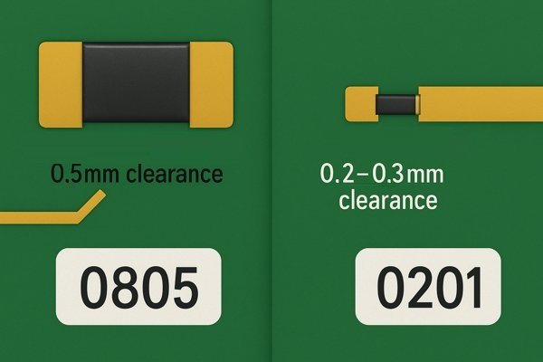
Smaller component packages require tighter spacing rules. While an 0805 component might be fine with 0.5mm (20 mils) clearance, a tiny 0201 package often requires a reduced clearance of 0.2mm - 0.3mm (8-12 mils) to balance density with manufacturability and prevent defects.
The Impact of Package Size on Spacing and Manufacturing Costs
In my work on a next-gen infusion pump, we had to use some incredibly small components to meet the size constraints. The decision to use 0201 passives wasn't just a layout choice; it had cascading cost implications throughout the project. The challenge with smaller packages isn't just the pick-and-place accuracy (typically ±0.05mm). It's the entire process chain:
- PCB Fabrication Cost: Supporting 0201 packages requires finer features on the bare board. Solder mask dams between pads might need to be 0.075mm (3 mils) or less, which increases the PCB cost.
- Assembly Cost: Assembly houses charge more for placing components smaller than 0402. Their machines have to run slower and require more precise calibration.
- Inspection Cost: Standard Automated Optical Inspection (AOI) may not be sufficient. For reliable inspection of 0201 solder joints, you often need 3D AOI or even Automated X-ray Inspection (AXI)4, both of which are more expensive.
This table summarizes spacing recommendations and the manufacturing class they fall into:
| Component Package | Body Size (mm) | Min. Spacing | Manufacturing Class |
|---|---|---|---|
| 1206 | 3.2 x 1.6 | 0.6 mm | Standard |
| 0805 | 2.0 x 1.25 | 0.5 mm | Standard |
| 0603 | 1.6 x 0.8 | 0.4 mm | Standard |
| 0402 | 1.0 x 0.5 | 0.3 mm | Standard |
| 0201 | 0.6 x 0.3 | 0.2 mm | Advanced/Micro |
| 01005 | 0.4 x 0.2 | 0.15 mm | Advanced/Micro |
Choosing to use an 0201 package to save a fraction of a millimeter in space might seem like a win, but it can increase the total assembled cost of the board by 10-20%. As engineers, we have to weigh that trade-off between size and cost.
What Are The Typical Spacing Values Used By PCB Assembly Houses For Standard Vs. Advanced Manufacturing?
Struggling to figure out if your design is manufacturable? You've packed components tightly, but you're worried your assembly house will reject the design or charge you a fortune for "advanced" processing. You need to know the industry's real-world numbers.
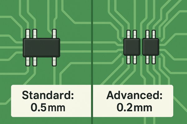
For standard manufacturing, most assembly houses recommend a minimum component-to-component spacing of 0.5mm (20 mils). For advanced or micro-assembly, this can be reduced to 0.2mm (8 mils) for the smallest packages, but this requires tighter process controls and often incurs higher costs.
Comparing Standard and Advanced Assembly Specifications
The difference between "standard" and "advanced" comes down to process capability and yield. Think of it in terms of a process capability index (Cpk)5. A standard process has a high Cpk (e.g., > 1.33), meaning it's highly repeatable and produces very few defects. An advanced process operates closer to the limits of the equipment, has a lower Cpk, and thus a naturally lower first-pass yield, which drives up the cost.
This table provides a clear comparison of capabilities:
| Parameter | Standard Manufacturing | Advanced Manufacturing |
|---|---|---|
| Component-to-Component | 0.5 mm (20 mils) | 0.2 mm (8 mils) or less |
| Min. Trace/Space | 0.127 mm (5 mils) | 0.075 mm (3 mils) or less |
| Via Technology | Tented/Untented Vias | Via-in-Pad, Microvias |
| Smallest Passive Component | 0402 | 0201 / 01005 |
| Relative Cost | Baseline (1x) | High (1.2x - 2x+) |
I once worked on a photonic computing chip evaluation board where the density was extreme. We had no choice but to use advanced assembly. We had to work closely with the assembly house, providing them with our design files early so they could run a detailed DFM analysis. This collaborative approach is essential when you're working on the advanced end of the spectrum.
How Do You Calculate The Clearance Between Different Types Of Components?
Calculating clearance feels complicated. Is it just one number for all components? Or does it change for a resistor next to a QFP? You need a simple, reliable method to get it right and avoid manufacturing issues.
The most reliable way is using the component courtyard method defined in IPC-7351B. Calculate the total clearance by adding the courtyard excess of component A to the courtyard excess of component B. For example, two components with a 0.25mm courtyard excess each require a total spacing of 0.5mm between their physical bodies.
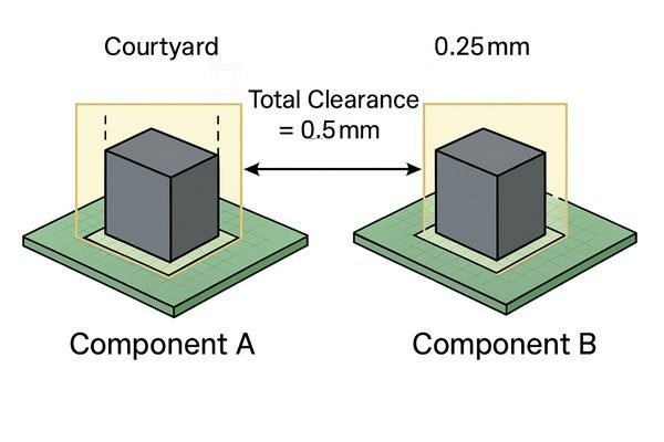
Calculating Spacing with the IPC Component Courtyard Method
The IPC courtyard method is the best practice because it standardizes the calculation. The formula is simply: Minimum Spacing = Courtyard Excess (Comp 1) + Courtyard Excess (Comp 2).
But what if your component library doesn't have courtyards defined? This is a common problem with downloaded or auto-generated footprints. In this case, you have to fall back to a manual calculation.
- Find the maximum extent of the land pattern (the pads). This is often called the "bounding box" of the copper.
- Add your desired courtyard excess to this bounding box. For Level B (Nominal), you would add 0.25mm on all sides. This becomes your effective courtyard.
- Now, place your components so that these manually-defined courtyard boundaries don't overlap.
Here are a few examples using the Level B (Nominal) density level:
| Component 1 | Component 2 | Courtyard Excess (C1) | Courtyard Excess (C2) | Required Spacing |
|---|---|---|---|---|
| 0603 Resistor | 0603 Resistor | 0.25 mm | 0.25 mm | 0.50 mm |
| 0603 Resistor | SOIC-8 IC | 0.25 mm | 0.25 mm | 0.50 mm |
| TQFP-100 | BGA-256 | 0.25 mm | 0.50 mm (for rework) | 0.75 mm |
Using courtyards in your design rules check (DRC) automates this process and is a system I rely on for every design to prevent placement errors before they happen.
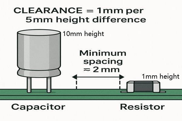
What Is The Minimum Spacing Between A Tall Component And A Short Component For Reflow Soldering?
Placing a tiny resistor next to a huge electrolytic capacitor is a common design problem. If you put it too close, you create problems for soldering, inspection, and rework. So what's a safe distance?
A good rule of thumb is to maintain a clearance of at least 1mm for every 5mm of height difference. For example, if a 10mm tall capacitor is next to a 1mm tall resistor (9mm difference), the minimum spacing should be nearly 2mm. This prevents shadowing during reflow and allows rework access.
Why Shadowing and Rework Access Dictate Tall Component Spacing
The issue with tall components like electrolytic capacitors, connectors, or inductors is twofold: the "shadow effect" during reflow soldering and the physical barrier it creates for inspection and rework. During reflow, a tall component can cast an IR "shadow" on a shorter one, leading to poor solder joints. For rework, a technician needs to get tools in there. A typical hot air nozzle has a diameter of 5-10mm, and AOI cameras need a clear line of sight at an angle of 30-45 degrees.
This practical guide helps determine spacing based on the height delta between adjacent parts:
| Component Height Difference | Minimum Recommended Clearance | Key Consideration |
|---|---|---|
| 0 - 2 mm | 0.5 mm | Standard placement |
| 2 - 5 mm | 1.0 mm | Allows AOI camera access |
| 5 - 10 mm | 2.0 mm | Ensures rework tool access |
| > 10 mm | 3.0 - 5.0 mm | Prevents significant IR shadowing |
This provides a good balance between layout density and the ability to actually build and repair the board.
What Are The Common Manufacturing Defects Caused By Incorrect Component Spacing?
You've submitted your design, but the assembly house reports low yields. The boards are plagued with shorts and open circuits. Often, the root cause isn't a bad component; it's spacing that was just a few mils too tight.
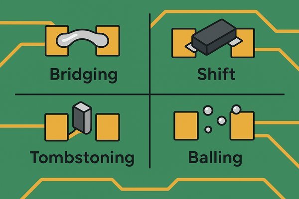
The most common defects from incorrect spacing are solder bridging (shorts between pads), component shifting, tombstoning, and solder balling. These issues directly result in failed boards, costly rework, and delayed production schedules.
From Solder Bridges to Tombstones: A Guide to Spacing-Related Defects
Manufacturing defects are where poor design choices become expensive realities. Here are the most common ones caused by improper spacing:
- Solder Bridging: This is the most frequent issue. It happens when solder merges between adjacent pads, creating a short. This is especially common with fine-pitch components when the solder mask dam between pads is less than about 0.1mm (4 mils).
- Component Shifting: The part moves from its intended position while floating on molten solder. If spacing is too tight, the surface tension from a neighboring component's solder can pull it out of alignment.
- Solder Balling: When pads are too close, solder paste can get squeezed out during component placement. This excess paste forms tiny balls during reflow that can detach later, creating intermittent shorts. This is a major reliability risk.
- Acid Traps: This is a PCB fabrication defect where acute angles in copper traces (< 90 degrees) trap etching chemicals, which can corrode the trace over time and cause a failure in the field.
This table summarizes the issues:
| Defect | Description | Primary Spacing-Related Cause |
|---|---|---|
| Solder Bridging | An unintended electrical connection (short) between two pads. | Insufficient solder mask dam (< 0.1mm) between adjacent pads. |
| Component Shift | Part moves from its intended position during reflow. | Surface tension from a neighbor's solder pulls the component. |
| Tombstoning | A two-terminal component stands up on one pad. | Thermal imbalance between the two pads causes uneven wetting. |
| Solder Balling | Small spheres of solder form on the board surface. | Solder paste squeezes out from between pads that are too close. |
| Acid Traps | Over-etching of copper at acute angles. | Traces routed at < 90° angles in tight spaces between pads. |
By providing enough room around each component, you give the manufacturing process the tolerance it needs to succeed.
How Is "Tombstoning" Related To Component Placement And Pad Design?
Have you ever seen a chip resistor standing up on one end like a tiny tombstone? This strange defect, aptly named "tombstoning," can bring your production to a halt. It's a classic sign that something is wrong with your layout.
Tombstoning occurs when the solder on one pad melts and pulls the component upright before the other pad's solder melts. This is caused by thermal imbalance, often due to one pad being connected to a large copper plane while the other has only a thin trace.
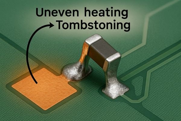
How Thermal Imbalance Causes Tombstoning
Tombstoning is a battle of surface tension forces. The number one cause is connecting one pad directly to a large copper plane, which acts as a heat sink and delays solder reflow on that pad. The solution is to ensure both pads reach reflow temperature at the same time.
Here are the do's and don'ts for preventing this defect:
| DO | DON'T | Reason |
|---|---|---|
| Use Thermal Reliefs on pads in planes. | Connect pads directly to a large copper plane. | Balances thermal mass and heat-up time. |
| Use Symmetrical Traces to pads. | Route a thick trace to one pad and a thin to another. | Ensures even heating of both pads. |
| Check Library Pads for symmetry. | Use footprints with significantly different pad sizes. | Prevents unbalanced solder paste volume. |
I make it a personal rule to review the connections to every two-terminal passive component, especially sizes 0402 and smaller, before finalizing a design.
What Is The Difference In Spacing Requirements For Reflow Versus Wave Soldering?
You’ve designed a board with parts on both sides. The top side will be reflowed, but the bottom side with through-hole parts will be wave soldered. Can you use the same spacing rules for both? Absolutely not.
Wave soldering requires significantly greater component spacing than reflow soldering. Components must be spaced far enough apart to prevent "solder shadowing," where a component blocks the solder wave from reaching the joints of a trailing component. A typical minimum is 2.5mm (100 mils).
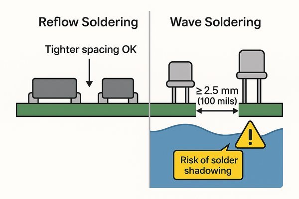
Why Wave Soldering Demands More Generous Spacing
Reflow soldering is a gentle, controlled process. Wave soldering is a dynamic, aggressive process where the board is dragged through molten solder. This fundamentally changes the design rules, especially regarding solder shadowing and component compatibility. Not all SMT components can survive the direct thermal shock of the solder wave.
| Parameter | Reflow Soldering | Wave Soldering |
|---|---|---|
| Min. SMT Spacing | 0.2mm - 0.5mm (8-20 mils) | ~2.5mm (100 mils) |
| Key Constraint | Solder Bridging | Solder Shadowing (components blocking solder flow) |
| Orientation | Low Concern | Critical; align similar parts parallel to the wave direction. |
| Component Concern | Thermal Profile | Thermal Shock & Component Compatibility (must be rated for wave) |
If you have a mixed-technology board, you must design the wave-soldered side with these much larger spacing rules and component compatibility in mind.
How Much Clearance Is Needed Between A Component And The Edge Of The PCB?
You've finished a dense layout, with components pushed right to the very edge of the board. But this can be a huge mistake, leading to damaged parts or a board that can't even be built.
A minimum of 3mm (120 mils) of clearance should be maintained between any component and the edge of the PCB. This "keepout" area is essential for automated handling, depaneling processes, and fitting the board into test fixtures.
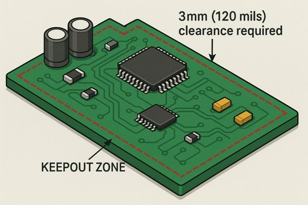
The Role of Edge Clearance in Assembly and Depaneling
The space at the edge of your board isn't empty; it's a vital part of the manufacturing process. Your board is manufactured in a large panel that needs a tooling frame for conveyor belts to grip. Fiducial markers for machine vision are also placed in this area. After assembly, the boards are separated (depaneled), which can stress nearby components.
The required clearance depends on the specific manufacturing step:
| Manufacturing Step | Reason for Clearance | Typical Clearance |
|---|---|---|
| Automated Handling | Gripping by conveyor belts in assembly machines. | 3.0 - 5.0 mm |
| V-Groove Depaneling | Stress from snapping can crack nearby solder joints. | > 1.25 mm from score line |
| Tab-Route Depaneling | Physical space needed for the router bit. | > 2.5 mm from routed edge |
| Test Fixtures | Space for guide rails and pogo pin mechanisms. | 3.0 mm |
I always create a "placement keepout" layer in my EDA tool for all board edges. For most designs, I use a 3mm keepout. If I know there are tall or sensitive components, like connectors, I increase that to 5mm.
What Is The Minimum Spacing Required Between A Component Pad And A Via?
You're routing a dense BGA and the only way out is to place a via right next to a pad. Do it wrong, and during reflow, the solder will get sucked off the pad and down into the via, creating a weak or open connection.
The minimum spacing between the edge of a component pad and the edge of a via's drill hole should be at least 0.15mm (6 mils) if the via is tented with solder mask. For untented vias, a larger spacing of 0.25mm (10 mils) is safer to prevent solder wicking.
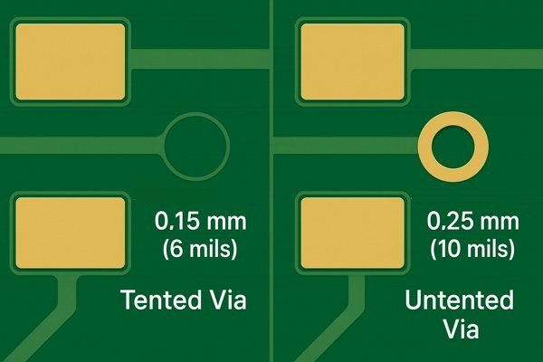
Preventing Solder Wicking with Proper Via Spacing and Treatments
The primary goal of via-to-pad spacing is to prevent "solder wicking." This is the capillary action that pulls molten solder off the pad and into the via barrel, starving the joint. The method you use to treat the via determines the required spacing and the cost.
| Via Treatment | Description | Min. Spacing to Pad Edge | Relative Cost |
|---|---|---|---|
| Tenting | Via covered with solder mask. | 0.15 mm (6 mils) | Baseline (1x) |
| Plugging | Via filled with non-conductive epoxy. | ~0.10 mm (4 mils) | Med (~1.1x) |
| Via-in-Pad | Via in the pad, filled and plated flat. | 0 mm | High (~1.25x) |
For most of my designs, I use tented vias and respect the 0.15mm (6 mil) rule. It provides the best balance of reliability and cost.
Are There Different Spacing Rules For Components On The Top And Bottom Sides Of The Board?
You've successfully designed a dense, single-sided board. Now you need to add components to the bottom. Can you just mirror the same design rules? Not quite. Double-sided assembly introduces new challenges that affect spacing.
Yes, the rules can differ. While the fundamental component-to-component spacing remains the same, you must account for the second reflow pass. Large, heavy, or sensitive components like fine-pitch BGAs should be placed on the side that is reflowed last (typically the top side).
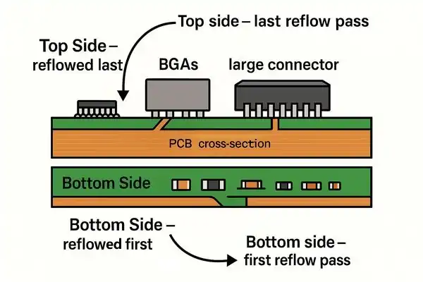
Placement Strategy for Double-Sided PCB Assembly
During the second reflow pass, the components on the first side are hanging upside down, held in place only by the surface tension of their re-melted solder joints. This creates critical placement constraints and dictates a clear strategy. For example, a fine-pitch BGA (< 0.8mm pitch) is at high risk of shifting or shorting if it's reflowed upside down.
This leads to a "Top-Side Heavy" design philosophy:
| Component Type | Recommended Side (Reflowed Last) | Reason |
|---|---|---|
| Heavy Components (>5g) | Top Side | Risk of falling off due to gravity during second reflow. |
| Fine-Pitch BGAs (<0.8mm) | Top Side | High risk of shorts or shifting due to weight and joint density. |
| Tall Connectors | Top Side | Can interfere with support pallets and cause shadowing. |
| Small Passives (0402/0603) | Bottom or Top Side | Low mass, held securely by surface tension. |
My strategy is to place all processors, BGAs, memory, connectors, and heavy magnetics on top. The bottom is for small passives and secondary ICs. This makes a huge difference in manufacturing reliability.
Conclusion
In short, successful PCB design isn't just about making circuits work; it's about making them manufacturable. Adhering to proper component spacing, from IPC standards to practical edge clearance, is a critical step.
-
Explore IPC-7351B to understand its significance in PCB design and how it can enhance manufacturability and repairability. ↩
-
Discover IPC-2221B to grasp the essential electrical clearance requirements that prevent arcing and ensure safety in designs. ↩
-
Explore the role of conformal coating in PCB design to learn how it can reduce spacing requirements and improve performance. ↩
-
Learn how AXI works and why it's crucial for inspecting tiny solder joints, ensuring quality and reliability in advanced electronics manufacturing. ↩
-
Understanding Cpk is crucial for improving manufacturing processes and ensuring quality control. ↩


