 Skip to content
Struggling with manufacturing defects slipping through? A lack of test points can cost you dearly in rework and delays. It's a common problem when testability isn't planned from the start.
There is no universal minimum number of test points. The goal is to achieve a specific test coverage, typically above 95%. For 100% electrical net coverage, every single net must have at least one test point accessible by the In-Circuit Test (ICT) fixture.
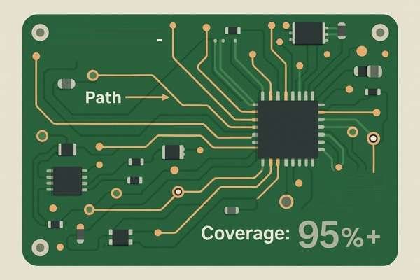
This simple answer, however, doesn't tell the whole story. Achieving high test coverage isn't just about adding points everywhere; it's about developing a smart and efficient strategy. Simply aiming for 100% on every design can lead to unnecessary complexity and cost, especially on dense boards. The real engineering challenge is to balance test coverage with design constraints like board space, signal integrity, and cost. Let's break down how to build a robust test point strategy that works in the real world.
What Components Or Nets Should Always Have Test Points?
Ever spent hours debugging a board, wishing you could just probe a critical signal? Forgetting a key test point turns a quick verification into a major headache, forcing you to solder wires or use expensive micro-probes.
Always add test points to power rails, ground, critical control signals (reset, enable), clock outputs, analog I/O, and programming interfaces like JTAG. These are non-negotiable for board bring-up, debugging, and production testing.
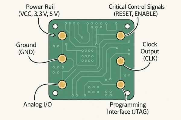
When I start a new layout, I have a standard checklist of nets that must get a test point, no matter how tight the board is. This isn't just for ICT; it's for my own sanity during the prototype phase. At Honeywell, on the Tuxedo Keypad project, we standardized this list across all product variants. This ensured that our test fixtures and debugging procedures were consistent, saving us countless hours.
Key Categories of Nets Requiring Test Points
A good way to organize your thinking is to group nets by function. This ensures you don't miss anything critical.
| Category | Rationale & Examples |
|---|---|
| Power & Ground | Essential for verifying that all ICs are powered correctly. Allows for checking voltage levels, noise, and current draw. Examples: +3.3V, +5V, VCC_CORE, GND. |
| Control Signals | These signals govern the state of the entire board. Being able to monitor and control them is vital for debugging. Examples: RESET_N, POWER_GOOD, ENABLE_3V3. |
| Clock Signals | Verifies that oscillators and clock distribution networks are functioning correctly. ICT can measure frequency and flag issues. Examples: SYS_CLK, XTAL_OUT, REF_CLK. |
| Analog I/O | Analog signals need to be measured for their precise voltage levels. Essential for sensor inputs, audio lines, and ADC/DAC references. Examples: ADC_IN, VREF, AUDIO_OUT. |
| Digital Interfaces | While JTAG can cover connectivity, test points are needed to check signal quality with a scope. Examples: UART_TX, I2C_SDA, SPI_MOSI. |
| Debug/Programming | Absolutely mandatory for flashing firmware and debugging the processor. Examples: JTAG_TCK, JTAG_TDO, SWD_CLK. |
It's important to expand on the "Digital Interfaces" point. You might think that if a bus is covered by JTAG, you don't need test points. But JTAG only tells you about connectivity (shorts and opens). It can't tell you about signal quality. If you are having intermittent issues on an I2C bus, you'll need to hook up an oscilloscope or logic analyzer to check for issues with rise times, voltage levels, or noise. Without a physical test point, this becomes nearly impossible. Adding one test point to SCL and SDA is a small price to pay for this critical debugging capability.
How Do You Develop A Comprehensive Test Point Strategy For A Complex Design?
Facing a dense, complex PCB? Deciding where to place hundreds of test points can feel overwhelming. A poor strategy results in low test coverage, untestable boards, and costly manufacturing problems down the line.
A comprehensive strategy starts by defining test coverage goals (e.g., 95%) with your manufacturer. Then, use Design for Test (DFT) software to analyze the netlist and automate initial placement, followed by a manual review to add crucial debugging points and resolve physical conflicts.

Developing a test point strategy is a formal process, not an afterthought. On the infusion pump project at Smiths Medical, reliability was paramount. Our process involved rigorous collaboration between hardware design, layout, and our contract manufacturer (CM) from day one. Here is the workflow we followed:
- Define Goals and Constraints: First, we decided on our test coverage target (99%+) and confirmed a single-sided (bottom) test methodology to control fixture costs.
- Collaborate with the CM: Before any placement, we had a technical discussion with our CM's test engineering team. This is a critical step. You must align on the specific capabilities and constraints of their equipment.
- Perform a Schematic-Level Analysis: We manually flagged all "must-have" test points (power, clocks, reset) directly in the schematic.
- Leverage DFT Automation Tools: We used the DFT tools in our EDA suite to automatically assign test points to all remaining uncovered nets.
- Review, Refine, and Document: Finally, we generated a coverage report, manually reviewed the automated placement, and documented everything in a formal Test Point Report.
Key DFT Parameters to Discuss with Your Manufacturer
This is the kind of specific information you need to discuss in Step 2 to avoid problems later.
| Parameter | Typical Value | Importance |
|---|---|---|
| Test Pad Diameter | 1.0mm (40 mils) | A larger pad provides a better target for the probe, increasing reliability. |
| Minimum Pitch | 1.91mm (75 mils) | A wider pitch reduces fixture cost and complexity. 1.27mm (50 mils) is possible but more expensive. |
| Pad-to-Component Clearance | 2.54mm (100 mils) | Prevents the test probe's body from hitting a nearby tall component. |
| Pad-to-Edge Clearance | 5.0mm (200 mils) | Allows the fixture's clamping mechanism to hold the board without interfering with probes. |
Is It Necessary For Every Net To Have A Test Point?
You're running out of space on a high-density board, and test points are taking up valuable real estate. You have to decide which nets to leave uncovered, but you're worried this will compromise testability and hide future problems.
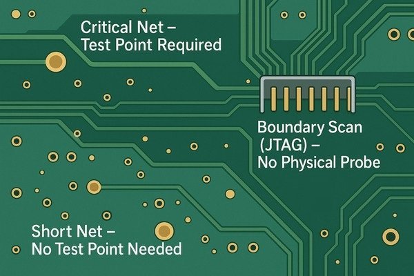
No, it is not always necessary for every net to have a test point. The goal is achieving adequate fault coverage. You can strategically omit points on non-critical or very short nets and use techniques like Boundary Scan (JTAG) to cover digital I/O pins without physical probes.
The philosophy of 100% test point coverage is becoming impractical. When I was debugging the photonic computing chip evaluation board at Lightelligence, many of the high-speed differential pairs were running at over 25 Gbps. Adding a test point stub would have ruined their signal integrity. Here’s how you can make smart trade-offs:
- Low-Impact Nets: Some nets are inherently low-risk. For example, a net that only connects a pull-up resistor to a nearby IC pin is very unlikely to have an open circuit. Many DFT tools can be configured to automatically ignore these "single-pin nets" or nets below a certain length (e.g., 5mm).
- Inferred Testing (Cluster Testing): Instead of testing every single net inside a simple functional block (like a power-on reset circuit), you can place test points at the inputs and outputs of the block. If the block behaves correctly when stimulated, you can infer that the internal connections are good.
- Nets Covered by Other Means: This is the most important category. Any net that is part of a JTAG chain can be tested for opens and shorts without a physical test point.
A Strategic Approach to Omitting Test Points
| Net Category | Rationale for Omitting Test Point | Alternative Test Method |
|---|---|---|
| High-Speed Digital | Stubs degrade signal integrity, causing reflections and data errors. | JTAG/Boundary Scan, Protocol-level tests (BERT1), Functional Test. |
| Short, Two-Pin Nets | Very low probability of an open circuit (e.g., a pull-up resistor to an IC pin). | Visual Inspection (AOI2), Inferred Testing. |
| Redundant Power/GND | Multiple pins connecting to the same plane. An open on one is unlikely to cause failure. | Test a few representative points on the plane. |
| Inaccessible Nets | Digital I/O pins between two BGAs. | JTAG/Boundary Scan is the only viable method. |
Focus on achieving 95%+ fault coverage, not 100% test point coverage. Your CM can use software like Valor NPI or Aegis FactoryLogix to generate a fault coverage report. This data-driven approach is far more effective.
Should Power And Ground Rails Have Multiple Test Points?
You've added a test point to your main 3.3V rail and one for ground. Is that enough? A single point confirms voltage is present, but it won't reveal potential issues with power distribution across a large, complex board.
Yes, absolutely. Power and ground rails should have multiple test points distributed across the PCB. This helps detect voltage drops (IR drop) and provides a stable, low-impedance return path for the ICT fixture.
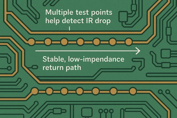
I learned this the hard way on an early industrial automation project. A board kept failing intermittently. A narrow trace feeding a high-current driver on the far side of the board was causing a significant voltage drop. For a sensitive component, that's a critical failure. For example, if a processor core rail requires 0.9V ±3%, that's only a 54mV total margin. On a 5A rail, just 10 milliohms of trace and via resistance will cause a 50mV drop, consuming almost your entire budget. Multiple test points would have caught this instantly.
Power and Ground Test Point Placement Guidelines
| Guideline | Specific Recommendation | Rationale |
|---|---|---|
| Geographic Distribution | Place test points in each quadrant of the board. | Provides a complete map of the power distribution network, revealing regional issues. |
| Proximity to Load | Place a test point near every high-current IC (CPU, FPGA, etc.). | Verifies the voltage delivered to the most critical components, accounting for IR drop. |
| Ground-to-Power Ratio | One ground test point for every 5-10 power test points. | Ensures the fixture has multiple, solid ground references for stable measurements. |
| Kelvin Sensing Support | For precision analog rails, provide a 4-point connection. | Allows for highly accurate voltage measurements by eliminating probe/trace resistance. |
What Specific Information About Test Points Should Be Included In The Fabrication And Assembly Notes?
Worried your CM will misinterpret your test plan? Ambiguous instructions lead to fixture errors and delays. Clear documentation is the only way to ensure a smooth handoff from design to manufacturing test.
Fabrication notes need a dedicated Gerber layer for test points, pad size specs (e.g., 1.0mm diameter), and clearances. Assembly notes require a Test Point Report file (in ASCII format) listing each point's ID, net name, and X-Y coordinates.

Clear communication with your partners is everything. You cannot assume the fixture house knows what you intended. Providing a complete and unambiguous data package is part of your job as a designer.
Checklist for Test Point Fabrication and Assembly Documentation
| Target | Required Information | Details |
|---|---|---|
| Fabrication | Dedicated Gerber Layer(s) | Create separate Gerber layers for top and bottom test points (e.g., Top_Test_Pads.gtp, Bottom_Test_Pads.gbp). |
| (PCB Shop) | Drill and Pad Specs | In your fab notes, clearly state the required finished size for test pads (e.g., "All test points shall be 1.0mm round pads"). Specify surface finish (e.g., ENIG). |
| Masking Instructions | Explicitly state that test points must be non-tented (solder mask opening must be larger than the pad). | |
| Assembly | Test Point Report / Centroid File | This is the most critical document. A simple text file (.txt or .csv) generated by your EDA tool containing: Test Point Name, Net Name, X-Y Coordinates, and Board Side. Include fiducial coordinates. |
| (CM/Fixture House) | Assembly Drawing Notes | Add a note on your assembly drawing: "Refer to Test Point Report file [filename].txt for ICT fixture locations." |
| Visual Diagram | Include a PDF showing the board layout with all test points clearly labeled. This serves as a human-readable cross-reference. |
What Are The Pros And Cons Of Using Test Points On The Top Versus The Bottom Side Of The PCB?
You need to add test points, but where should they go? Placing them on the top side seems convenient for manual debugging, but your CM says all test points must be on the bottom. Understanding the trade-offs is key to avoiding costly fixture designs.
The bottom side is the industry standard for automated ICT fixtures because it simplifies fixture construction and cost. The top side is better for manual probing during development and debug. Placing points on both sides requires a complex and expensive "clamshell" fixture.
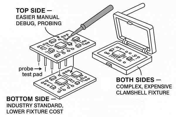
I've worked on designs that required a clamshell fixture. The fixture cost was more than double that of a single-sided one, and the mechanical complexity led to more frequent maintenance. The rule is simple: keep all automated test points on one side, preferably the bottom, unless it's absolutely impossible.
Comparing Top-Side vs. Bottom-Side Test Point Placement
| Feature | Top Side Placement | Bottom Side Placement |
|---|---|---|
| Automated Testing | Con: Requires an expensive clamshell fixture. Increases cost, complexity, and setup time. | Pro: Standard industry practice. Allows for a simple, low-cost, single-sided fixture. |
| Manual Debugging | Pro: Excellent accessibility for probing with an oscilloscope while the board is operating. | Con: Poor accessibility. You have to flip the board over to probe. |
| Component Density | Con: Competes for space with components, connectors, and labels. Can be blocked by heat sinks or shields. | Pro: The bottom side is often less populated, leaving more room. |
| Reliability | Con: A two-sided fixture has more moving parts and twice the number of probes, increasing points of failure. | Pro: Simpler mechanical design leads to higher reliability in high-volume production. |
How Does Adding A Test Point Stub Affect Signal Integrity On High-Speed Nets?
Designing a high-speed bus? Adding a test point feels like a risk. That extra trace stub can create reflections and ruin your signal integrity, causing mysterious data errors that are difficult to debug.
A test point stub adds parasitic capacitance (typically 0.5 pF to 1.0 pF) and acts as an unterminated transmission line. This creates an impedance discontinuity that causes signal reflections, degrading signal integrity on nets operating above a few hundred MHz.
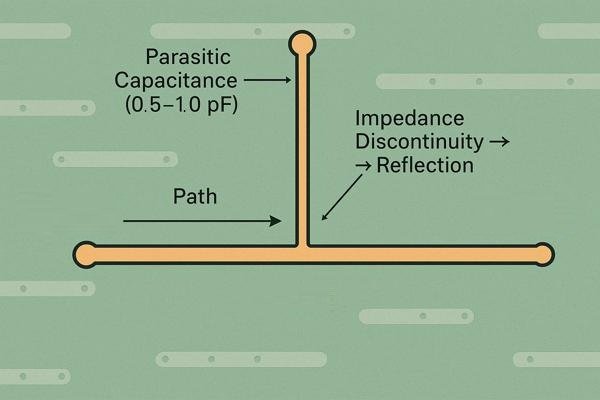
For high-speed design, you must treat test points as electrical components. A common rule is that the stub's electrical length should be much less than the signal's rise time, typically less than 1/6th of the rise/fall time. For a signal with a 100 ps rise time, your stub needs to have a delay under ~16 ps, corresponding to only about 2-3 mm of trace length. Here are the best ways to manage this:
- Keep Stubs Extremely Short: The trace connecting the main signal path to the test pad should be as short as physically possible.
- Use Vias as Test Points: Instead of branching off a trace to a dedicated pad, place the test point directly on a via in the signal path. Probing the via itself results in the smallest possible stub. For the highest speeds, you can specify back-drilling the unused portion of the via to remove its capacitive stub.
- Place Stubs at the End of the Line: If you must have a stub, locate it at the receiver end of the transmission line, not in the middle.
- Simulate, Simulate, Simulate: Use a signal integrity simulator like Ansys SIwave or Cadence Sigrity. These tools allow you to add a model for your test point and see its exact impact on the eye diagram.
High-Speed Test Point Mitigation Techniques Summary
| Technique | Description | Best For... |
|---|---|---|
| Minimal Length Stubs | Keep the trace from the main line to the test pad as short as physically possible. | Signals up to ~1-2 Gbps. |
| Via-as-Test-Point | Place the test point directly on a signal via instead of a separate pad. Specify back-drilling for ultimate performance. | Any high-speed signal, especially differential pairs. |
| End-of-Line Placement | Locate the test stub at the receiver end of the transmission line. | Minimizing multiple reflections on a point-to-point bus. |
| Simulation | Model the test point (pad + stub) in an SI simulator to quantify its impact on the eye diagram. | All critical high-speed interfaces (e.g., DDR, PCIe). |
What Are The Best Practices For Testability In High-Density Interconnect (HDI) Board Designs?
Working with HDI and 0.4mm BGAs? Traditional test points won't fit. You're worried your board will be a "black box" that is impossible to test or debug in production.
For HDI, use smaller test pads (e.g., 0.5mm), leverage microvias as test access points, and heavily rely on JTAG for BGA I/O coverage. Prioritize flying probe testing over expensive and fragile bed-of-nails fixtures for fine-pitch designs.
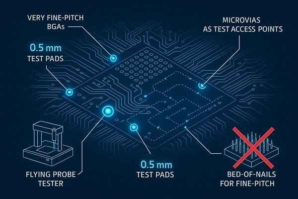
HDI design forces a complete shift in test strategy. The old rules of "a test point on every net" no longer apply. You must design for testability using a combination of modern techniques.
HDI Testability Best Practices
| HDI Challenge | Best Practice Solution | Key Considerations |
|---|---|---|
| Lack of Space | Use microvias in BGA fanouts as test points. Miniaturize pads to 0.3mm - 0.5mm. | Vias must be untented. Requires a flying probe tester capable of high precision. |
| Inaccessible Pins | Implement a robust JTAG/Boundary Scan strategy. | JTAG is mandatory for connectivity tests on any BGA with a pitch ≤ 0.8mm. |
| High Fixture Cost | Use flying probe testing instead of a bed-of-nails fixture. | Ideal for prototypes and low-to-mid volume. Slower cycle time than ICT. |
| Hidden Solder Defects | Require Automated X-Ray Inspection (AXI)3 after assembly. | AXI is critical for finding shorts, voids, and misalignments under BGAs. |
Are There Special Considerations For Placing Test Points On RF Or Impedance-Controlled Traces?
Need to test an RF signal? Placing a test point directly on an impedance-controlled trace can detune the entire circuit, causing massive signal reflections and performance loss. You need a way to probe without disrupting the system.
Never place a test point directly on an RF or impedance-controlled trace. Instead, use a coupling capacitor or a series resistor (often 0-ohm) to create a test spur that isolates the probe's capacitance from the main transmission line.
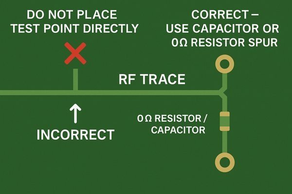
I learned this while working on a Wi-Fi module redesign. A test pad placed directly on the 50-ohm trace to the antenna completely detuned the matching network. The solution was to create an isolated test spur. Here are the common methods:
- Capacitive Coupling4: A small, secondary trace branches off the main RF line and ends in an unpopulated SMT capacitor pad (e.g., 0402). The other side of this footprint connects to your test pad.
- Resistive Tap: A spur branches off the main line to a 0-ohm resistor footprint, followed by the test pad. The resistor is only populated for testing.
- Dedicated RF Probe Points (GSG): For precision VNA measurements, the best method is to design a Ground-Signal-Ground (GSG) footprint directly on the board.
Comparison of RF Probing Methods
| Method | How It Works | Pros & Cons |
|---|---|---|
| Capacitive Coupling | A spur leads to an unpopulated capacitor footprint, then to a test pad. | Pro: Provides AC coupling. Good for in-band signal checks. Con: Blocks DC bias. |
| Resistive Tap | A spur leads to a 0-ohm resistor footprint, then to a test pad. | Pro: Simple, passes DC. Can use non-zero values for attenuation. Con: Can load the line if not a high impedance tap. |
| GSG Probe Point | A dedicated Ground-Signal-Ground footprint designed for direct VNA probing. | Pro: Highly accurate, calibrated, impedance-matched measurements. Con: For lab use only, not for production ICT. |
From A Designer's Perspective, When Does It Make Sense To Use Boundary Scan (JTAG) Instead Of Physical Test Points?
Your board is covered in BGAs with hundreds of hidden pins. Using physical test points for every I/O is impossible. You need a reliable way to confirm thousands of connections without a thousand-pin test fixture.
Use JTAG to test the connectivity between complex digital ICs (FPGAs, CPUs, ASICs), especially for pins hidden under BGA packages. It is ideal for detecting shorts, opens, and missing pull-up/down resistors on digital nets that are physically impossible to probe.
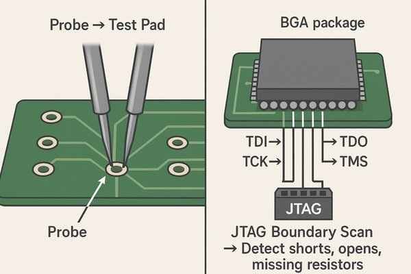
JTAG is not a replacement for ICT, but a complementary technology. ICT is like using a multimeter, while JTAG is like asking the chips themselves to report if their connections are good. This requires getting the BSDL (Boundary Scan Description Language)5 file for each IC in the chain from the manufacturer, which describes the IC's boundary scan logic.
JTAG vs. ICT: Choosing the Right Tool
| Aspect | Boundary Scan (JTAG) | In-Circuit Test (ICT) |
|---|---|---|
| Primary Use Case | Testing digital connections between JTAG-compliant ICs. | Testing all electrical nets for shorts/opens and verifying analog component values. |
| Limitations | Cannot test timing, signal integrity, or non-JTAG parts. | Cannot access pins under BGAs. Test stubs can affect high-speed signals. |
| Physical Access | Only needs access to the 4-5 JTAG port pins. | Requires a physical test pad for every net being tested. |
| Fixture Cost | Very low. Only requires a JTAG programmer. | High. Custom bed-of-nails fixtures can cost thousands of dollars. |
What Design Features Are Needed To Support A Combined In-Circuit Test (ICT) And Functional Circuit Test (FCT)?
Your product needs both ICT and FCT to guarantee quality. How do you design a board that supports both without creating a fixture nightmare? The key is to plan for both test stages from the beginning.
For a combined test, design for ICT access on the bottom side (test points) and provide FCT access to all user I/O (connectors, LEDs, buttons) through a consolidated test header or edge connector, enabling a two-stage fixture.
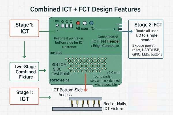
On the Tuxedo Keypad, our fixture was a two-stage design. The first stage ran ICT. If that passed, the second stage engaged the keypad and LCD connectors, powered up the device, and ran a functional script. This combined approach allowed us to catch 99% of all possible defects in a single test step.
Combined ICT/FCT Design Features Checklist
| Design Area | Required Feature | Purpose |
|---|---|---|
| Physical Layout | Consolidate FCT I/O to a dedicated connector or edge pads. | Simplifies fixture mechanics, reducing cost and improving reliability. |
| Electrical | Allow fixture to control main power and reset lines. | Enables the fixture to safely power cycle the board and run test sequences from a known state. |
| Electrical | Use jumpers or multiplexers to isolate circuit sections. | Allows ICT to test sections without interference from other active components. |
| Firmware | Make the JTAG/SWD port accessible to the fixture. | Allows a special test firmware to be loaded before FCT begins. |
| Firmware | Provide a fixture-controlled pin to disable watchdog timers. | Prevents the board from resetting during long test sequences. |
Conclusion
Ultimately, the right number of test points is the number that gives you confidence in your product's quality without compromising its design or budget.
-
Learn how BERT helps verify signal integrity and data reliability in high-speed digital designs, crucial for avoiding errors without physical test points. ↩
-
Learn how AOI helps detect assembly defects and ensures quality in PCB production, making it a valuable alternative to physical test points. ↩
-
This link will provide insights into how AXI enhances quality control by detecting hidden defects in assemblies. ↩
-
Explore this link to understand how capacitive coupling can enhance your RF design and testing methods. ↩
-
Understanding BSDL is crucial for effective JTAG implementation, as it defines the boundary scan logic for ICs. ↩


