 Skip to content
Struggling with manufacturing holds on your PCB design? These delays often come from simple mistakes like improper edge clearance, causing frustrating back-and-forth communication that can derail your project schedule.
Most PCB manufacturers require a minimum trace-to-board-edge clearance of 0.25mm to 0.3mm (about 10 to 12 mils) for routed boards. This "safe" distance prevents copper features on external layers from being exposed or damaged during the depaneling process.
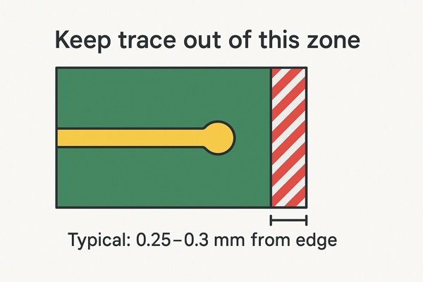
Getting your board made right the first time is about more than just a good schematic. These small manufacturing rules are what separate a successful prototype from a costly coaster. The table below provides a quick summary of the most common edge clearance requirements, which we will explore in detail.
| Feature | Minimum Clearance from Board Edge | Primary Reason |
|---|---|---|
| External Traces/Pads | 0.25 mm (10 mils) | Prevent exposure during routing/depaneling. |
| External Copper Pours | 0.50 mm (20 mils) | Avoid shorts and ensure solder mask adhesion. |
| Internal Layer Copper | 1.0 mm (40 mils) | Prevent internal shorts from copper smearing. |
Let's dive deeper into the specifics for each of these rules.
What Is the Required Clearance for a Copper Pour to the Board Edge?
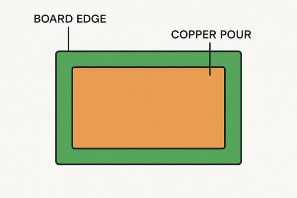
You’ve flooded your layout with a ground pour for shielding. But if it creeps too close to the edge, it can cause shorts, peeling, and fabrication failures during depaneling.
For a copper pour, the standard minimum clearance to the board edge is 0.5mm (about 20 mils). This is typically larger than the clearance required for a single trace because of the greater risk of shorting along a continuous metal edge.
Preventing Shorts from Routing Tolerances
A single trace is a small feature. If a router bit deviates slightly, it might nick a trace, but a large copper pour presents a much bigger target. A copper pour creates a long, continuous metal edge. When the board is routed out of the main panel, any slight deviation in the router path could expose this edge along a significant length. This exposed copper can then easily short to a metal enclosure, another PCB, or even a person's hand. In my experience with the Tuxedo Keypad, we had to be extremely careful with this, as the board sat right against a plastic housing with metal clips. An exposed ground pour could have created an intermittent shorting path when the device was handled.
Ensuring Plating Uniformity and Solder Mask Adhesion
Beyond shorting risks, pulling copper pours back from the edge is also critical for plating quality. Large copper areas act as "plating thieves," drawing more current during the electrolytic plating process. If a large pour is too close to the edge, it can cause the copper thickness on the rest of the board to be uneven. Pulling it back promotes a more uniform current density and consistent plating. Furthermore, this clearance provides a solid, copper-free surface for the solder mask to adhere to. Without this "solder mask dam," the mask can peel away at the edge during handling or thermal cycling, exposing the copper you were trying to protect.
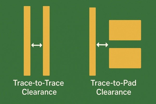
What Are the Standard Minimums for Trace-to-Trace and Trace-to-Pad Clearance?
Trying to pack your design as tightly as possible is a common goal. But if you place traces too close to each other or to pads, you risk shorts during etching and assembly, crosstalk, and poor fabrication yields.
For standard, cost-effective manufacturing, a trace-to-trace and trace-to-pad clearance of 0.15mm / 0.15mm (6 mils / 6 mils) is a very common and safe baseline. While many advanced manufacturers can achieve 0.1mm / 0.1mm (4 mils / 4 mils) or less, sticking to wider spacing improves yield and lowers cost.
How Voltage Dictates Clearance According to IPC-2221B1
The minimum clearance is dictated by electrical safety standards, not just manufacturing capability. IPC-2221B provides specific guidance on the required spacing between conductors based on peak voltage.
Here's a simplified table based on IPC-2221B (Level B2) for conductors at altitudes up to 3,050 meters. Note the distinction between external and internal layers.
| Peak Voltage | External Clearance (Coated) | Internal Layer Clearance | Common Practice (External) |
|---|---|---|---|
| 0 - 15V | 0.05 mm (2 mils) | 0.05 mm (2 mils) | 0.127 mm (5 mils) |
| 16 - 30V | 0.05 mm (2 mils) | 0.05 mm (2 mils) | 0.127 mm (5 mils) |
| 31 - 50V | 0.10 mm (4 mils) | 0.05 mm (2 mils) | 0.20 mm (8 mils) |
| 51 - 100V | 0.10 mm (4 mils) | 0.05 mm (2 mils) | 0.25 mm (10 mils) |
| 101 - 250V | 0.20 mm (8 mils) | 0.10 mm (4 mils) | 0.40 mm (16 mils) |
Using Clearance to Control Crosstalk in High-Speed Designs
For high-speed designs, clearance is about more than just preventing shorts; it's about managing electromagnetic fields. The spacing between traces is a critical factor in controlling crosstalk (unwanted noise coupling). For differential pairs, the spacing between the two traces is tightly controlled to maintain a specific impedance (e.g., 100Ω). Likewise, the clearance from these pairs to adjacent signals must be increased, often to 3x or 5x the trace width (the "3W rule"), to prevent the fields from interfering and corrupting your signal. In this context, clearance becomes a signal integrity tool, not just a manufacturing rule.
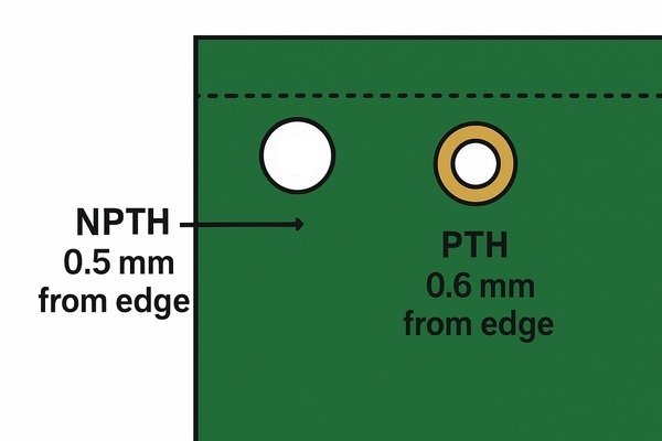
What Is the Minimum Required Distance from a Drill Hole to the Board Edge?
Placing a mounting hole or via right at the board's edge seems like an efficient use of space. This can lead to hole breakout, where the drill bit cuts into the board edge, cracking, and structural weakness.
For a non-plated (NPTH) drill hole, the minimum distance from the hole's edge to the board edge is typically 0.5mm (20 mils). For a plated (PTH) drill hole, this distance should be larger, around 0.6mm (24 mils), to ensure the integrity of the plating barrel.
Why Plated Holes (PTH) Require More Clearance Than Non-Plated (NPTH)
A non-plated hole is just a mechanical feature. It needs enough surrounding FR-4 material to avoid cracking under stress. A plated-through hole (PTH), however, is an electrical connection. The plating inside the barrel needs a solid copper pad—the annular ring—to anchor to. If the drill wanders and removes part of this ring ("breakout"), the electrical connection can be compromised. This is why PTHs demand a greater setback, as summarized below.
| Hole Type | Minimum Clearance (Hole Edge to Board Edge) | Key Consideration |
|---|---|---|
| Plated (PTH) | 0.6 mm (24 mils) | Must preserve the copper annular ring for plating integrity. |
| Non-Plated (NPTH) | 0.5 mm (20 mils) | Needs enough board material to prevent cracking. |
Increasing Clearance for Press-fit Connectors and Countersunk Holes
The rules get stricter for special hardware. Press-fit connectors, for instance, are forced into plated holes and exert enormous stress on the board. Placing one too close to an edge is a recipe for delamination and board fracture. For these, I always consult the connector's datasheet and typically add an extra 1-2mm of clearance beyond the standard minimum. Similarly, if your design requires secondary operations like counter-boring or counter-sinking for flat-head screws, you must account for the larger diameter of this secondary drill and ensure even more clearance to the board edge.
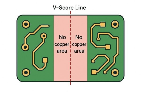
How Does V-Scoring Impact Edge Clearance Requirements?
Using V-scores is an efficient way to panelize boards for mass production. However, the scoring process itself removes material and can easily expose copper if your traces or pours are too close to the line.
To safely accommodate V-scoring, all copper features (traces, pads, and pours) should be kept at least 0.4mm (16 mils) away from the center of the V-score line. Some high-volume manufacturers may even recommend 0.5mm (20 mils) for better results.
How a V-Groove's Structure Affects Nearby Copper
A V-score is a V-shaped groove cut into the top and bottom surfaces, typically leaving a thin web of material (about 1/3 of the board thickness) in the middle. The board is snapped along this weakened line. The cutting tool has a tolerance and can wander. Furthermore, the snapping action is a fracture, not a clean cut, which can create a rough edge and put stress on nearby features. The table below outlines key design rules.
| V-Scoring Design Parameter | Recommended Value | Rationale |
|---|---|---|
| Copper to V-Score Centerline | ≥ 0.4 mm (16 mils) | Prevents copper exposure from tool wander and fracturing. |
| Min. Board Thickness | ~0.8 mm (32 mils) | Thinner boards may break during assembly. |
| Remaining Web Thickness | ~1/3 of total board thickness | Provides a balance of stability and ease of snapping. |
Using Jump-Scoring to Create a Smooth Board Edge for Connectors
What if you have an edge-card connector that must be perfectly flush with the board edge? You can't have a V-score run through it. In this case, we use "jump-scoring," where the scoring tool lifts and "jumps" over a specific area, leaving that section of the edge smooth and uncut. When designing for this, you must manage the transition. The copper clearance rule of 0.4mm applies right up to the point where the score stops, and then it can revert to the standard 0.25mm clearance for the routed/un-scored section. It requires careful design and clear communication with your fabricator.
How Does Tab Routing Impact Edge Clearance Requirements?
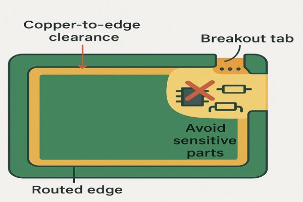
Tab routing is another popular method for panelizing boards, especially for non-rectangular shapes. The routed channels and breakout tabs create their own set of clearance rules you must follow.
For tab-routed designs, the standard copper-to-edge clearance of 0.25mm to 0.3mm (10 to 12 mils) applies, measured from the routed edge. Additionally, it is critical to keep sensitive components and traces away from the breakout tabs themselves due to mechanical stress during depaneling.
Defining Keep-Out Zones to Prevent Stress Fractures at Tabs
Where you place your tabs matters. Don't just let the fab house decide for you. For optimal results, specify tab locations in your fabrication drawing. Distribute them evenly on straight edges to provide panel stability during assembly. Most importantly, never place a tab directly next to a sensitive component (like a crystal or ceramic capacitor) or a critical connector. The shock of breaking the tab can fracture solder joints or damage the component itself. I always define a keep-out area of at least 1.25mm (50 mils) around breakout tabs and ensure they are placed on the most robust parts of the board outline. Choosing between V-scoring and tab routing depends on your design's specific needs.
| Feature | V-Scoring | Tab Routing |
|---|---|---|
| Best For | Rectangular boards in high-volume production. | Irregularly shaped boards or panels with mixed designs. |
| Board Edge Finish | Rough, fractured edge. | Smooth, routed edge (with minor blemishes at tabs). |
| Stress on Board | High stress along the entire score line. | Stress is localized to the breakout tab locations. |
| Usable Board Area | Loses ~0.4mm along the edge to clearance. | Loses space for the routed channel (~2mm) between boards. |
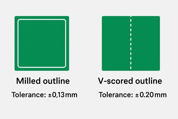
What Are Typical Manufacturing Tolerances for a PCB Board Outline?
You’ve designed a PCB to fit perfectly into a custom-milled enclosure. But if you don’t account for the board fabricator's manufacturing tolerances, you might find your board is too big to fit or rattles around.
For a standard mechanically routed (milled) PCB outline, a typical manufacturing tolerance is ±0.13mm (±5 mils). For boards separated by V-scoring, the tolerance can be higher, often in the range of ±0.2mm (±8 mils) due to the less precise nature of snapping.
Using Clearance as a Buffer Against Outline Tolerances
No manufacturing process is perfect. This ±0.13mm tolerance is precisely why we have clearance rules. The 0.25mm copper-to-edge clearance acts as a vital buffer. It ensures that if the router cuts 0.13mm deeper than intended, your copper trace is still a safe 0.12mm away from the physical edge. When designing for tight-fitting assemblies, you must account for this in your mechanical CAD model. I always design my enclosures with an extra gap of 0.2mm to 0.3mm beyond the nominal board dimensions to accommodate the worst-case tolerance stack-up.
Tighter Tolerances with Laser Cutting and Panel Considerations
For applications requiring extreme precision, the fabrication method determines the achievable tolerance.
| Fabrication Method | Typical Dimensional Tolerance | Best Use Case |
|---|---|---|
| V-Scoring | ±0.2 mm (±8 mils) | High-volume rectangular boards where edge finish is not critical. |
| Routing/Milling | ±0.13 mm (±5 mils) | Standard for most designs, including irregular shapes. |
| Laser Cutting | ±0.05 mm (±2 mils) | High-precision, flex/rigid-flex circuits, or sensitive materials. |
It's also important to remember that across a large production panel, tolerance can be cumulative. The first board in the panel might be nearly perfect, while the last board might exhibit the maximum deviation. This is a factor to discuss with your manufacturer when planning for high-volume production.
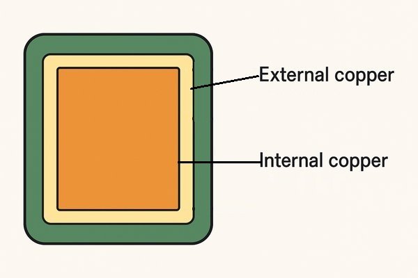
Are Edge Clearance Requirements for Internal Copper Layers Different from External Layers?
It's easy to focus on the external layers that you can see. However, internal copper layers also have critical edge clearance requirements that, if ignored, can lead to catastrophic failures.
Yes, the edge clearance for internal copper layers is different and almost always larger than for external layers. A standard requirement is for all internal copper to be pulled back 1.0mm (about 40 mils) from the routed board edge.
Preventing Internal Shorts Caused by Copper Smearing During Routing
This rule exists to prevent copper smearing. When a router bit cuts through a multilayer PCB, the heat and friction can drag small particles of copper from the internal planes along the board edge. If your internal ground and power planes are too close to the edge, this smearing can create a conductive path between them, resulting in a permanent, low-impedance short circuit that is impossible to see or fix. Pulling the internal copper back by 1.0mm creates a robust FR-4 buffer zone, making this failure mode physically impossible. For high-reliability applications, this is non-negotiable.
How Internal Plane Pullback Affects High-Frequency Edge Resonance
This pullback also has a secondary, high-frequency effect. The edge of a parallel power and ground plane pair can act like a slot antenna, radiating noise at specific resonant frequencies. While the 1.0mm pullback is primarily for anti-smearing, it also slightly alters this resonant behavior. In ultra-high-speed designs, engineers sometimes use techniques like edge plating or "via stitching" around the board perimeter to control this edge radiation, but for most designs, the standard pullback is the most important rule to follow.
What Are the Design Considerations for Castellated Holes on a Board Edge?
Castellated holes are an excellent feature for creating modules that can be soldered directly onto a parent board. But designing them incorrectly is a common source of manufacturing problems and poor solder joints.
A successful castellated hole requires a pad that extends sufficiently onto the PCB, a proper annular ring for the plated half-hole, and adequate spacing between castellations. The hole must be defined as a plated-through hole (PTH) that is intentionally cut by the board outline routing path.
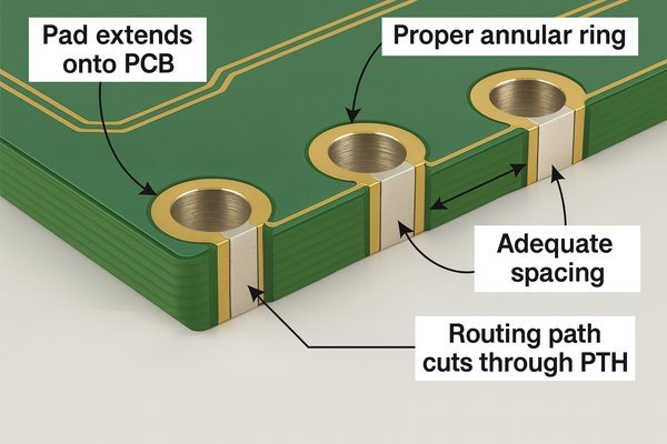
Defining Pad and Drill Parameters for Manufacturability
Designing robust castellated holes requires attention to a few specific parameters. The process involves drilling, plating, and then precisely routing through the center of the holes.
| Parameter | Guideline | Reason |
|---|---|---|
| Placement | Center the PTH directly on the board outline. | To create a clean, semi-circular half-hole. |
| Drill Size | 0.5mm to 0.8mm is common. | Balances manufacturability with solder fillet formation. |
| Pad Size | At least 2x the drill diameter. | Ensures a sufficient annular ring after routing. |
| Pad Extension | Extend pad at least 0.5mm into the PCB. | Provides a solid landing area for soldering. |
| Spacing | Keep at least 0.6mm between edges of pads. | Prevents solder bridging between castellations. |
Improving Solderability with Surface Finish and Direct Thermal Connections
For the most reliable solder joints on castellated holes, the surface finish matters. I strongly recommend Electroless Nickel Immersion Gold (ENIG)2 because it provides a perfectly flat, highly solderable surface. Hot Air Solder Leveling (HASL)3 can leave an uneven surface on the half-hole, making consistent mounting difficult. Additionally, if the castellated pad connects to a large ground or power plane, use a direct connection instead of thermal reliefs. While this makes manual soldering harder, it is essential for ensuring the pad gets hot enough during reflow to form a strong, complete solder fillet. A thermal relief can starve the pad of heat, resulting in a weak or cold joint.
Conclusion
Following PCB manufacturing clearances isn't about limiting your design. It’s about embracing Design for Manufacturability (DFM) to ensure your projects are delivered on time and on budget without needless delays.
-
Exploring IPC-2221B will provide insights into essential electrical safety standards and clearance requirements for conductors. ↩
-
Explore the advantages of ENIG for solderability and reliability in PCB designs. ↩
-
Learn about HASL's impact on solder joint quality and its suitability for different applications. ↩


