 Skip to content
Your prototype passes every test on the bench, but fails EMI compliance. Worse, it has intermittent failures in the field. You've checked every component, but the mysterious glitches and noise persist, threatening your entire project timeline. The culprit is often a misunderstood return current; let's master its behavior to build truly robust designs.
A return current is the flow of electrons completing a circuit by traveling back to the voltage source. On a PCB, this current doesn't just vanish into "ground." It actively seeks the path of least impedance. If this path is poorly designed, it causes crosstalk, EMI, and other issues.
In my nearly 20 years as a hardware engineer, I've seen more projects delayed by return path problems than almost any other issue. An engineer designs a perfect schematic, the simulation looks great, but the physical board is a noisy mess. This happens because the layout, not the schematic, defines the return path. Understanding the physics of this path—how it changes with frequency and how to control it—is what separates a functional prototype from a reliable, mass-produced product. Let's break down this crucial concept so you can avoid these costly and frustrating mistakes.
What is the difference between ground and a return path?
You’ve diligently connected all your GND pins to a solid ground plane, yet your circuit is noisy. You assume "ground is ground," but this common simplification is causing high-speed signals to radiate and interfere with each other. The key is understanding that "ground" is a reference, while the "return path" is a physical route that you must design carefully.
"Ground" is simply a reference point in a circuit, defined as \(0\text{V}\). A "return path" is the physical conductor—a trace or a plane—that the current actually travels on to get back to its source. The current’s goal is to complete its loop back to the source, not just to reach "ground."
When Return Paths Go Wrong
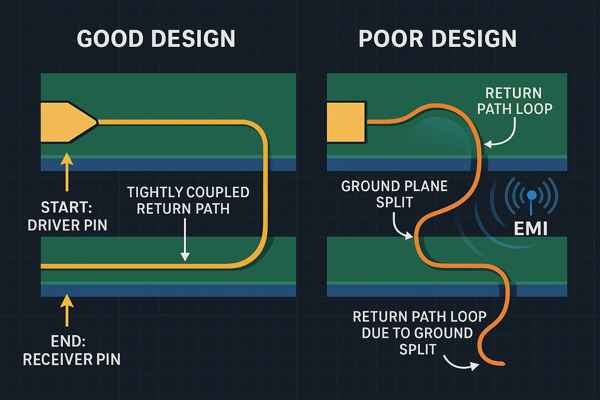
The most dangerous mistake is assuming a ground plane is a magical carpet that makes return currents disappear. A classic error is routing a high-speed signal trace across a split in a ground plane, which forces the return current on a long detour. This creates a massive current loop that acts as an antenna, almost guaranteeing an EMC failure.
| Concept | Definition | Purpose in a Circuit |
|---|---|---|
| Ground (\(\text{GND}\)) | An electrical reference point, typically defined as \(0 \text{ Volts}\). | Provides a common voltage reference for all signals, ensuring components operate correctly relative to each other. |
| Return Path | The physical conductive path the current follows to flow from the load back to the source. | Completes the electrical circuit. Its physical layout is a primary factor in signal integrity, crosstalk, and EMI performance. |
These conceptual misunderstandings lead to concrete design errors. I've seen these mistakes cost weeks of debugging and thousands of dollars in board re-spins.
| Common Return Path Error | Consequence | Why it Happens |
|---|---|---|
| Routing over a Split Plane | High radiated emissions (EMI), signal degradation. | Forces the high-frequency return current into a large loop, creating an efficient antenna. |
| Changing Layers without a Return Via | Signal reflections, crosstalk. | The return current is stranded on the original reference plane and has to find a distant path (e.g., a decoupling cap) to switch layers. |
| Excessive Voids in a Plane | Inconsistent impedance, increased noise. | Voids (from too many vias) can create detours and "swiss cheese" planes, forcing return currents on longer, higher-inductance paths. |
| Sharing Vias for Decoupling and Return | High-frequency noise coupling. | A via should provide a direct path. Sharing it can inject noise from one part of a circuit directly into the return path of another. |
Why does current follow the path of least resistance at DC?
You have a power plane that looks solid, but a component at the far end of the board is resetting randomly. This instability, caused by voltage drop (\(IR\) drop), can be a nightmare to diagnose, as it might only occur under heavy load. Let's examine why DC current follows the path of least resistance and how to design for it to ensure stable power delivery.
At DC (a frequency of \(0 \text{ Hz}\)), a circuit's behavior is governed only by resistance. Current will distribute itself across all available paths, but the highest concentration of current will flow through the path that offers the lowest total resistance, as dictated by Ohm's Law (\(V=IR\)).
The Impact of I*R Drop
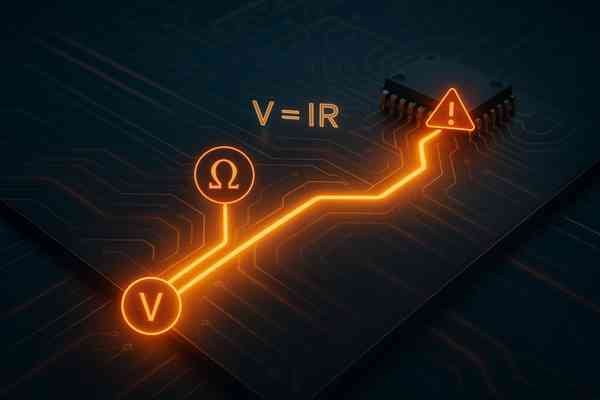
At DC, the only thing opposing current flow is resistance. No conductor has zero resistance, and this becomes a big problem when significant current flows through it. According to the formula \(V = IR\), even a small resistance (\(R\)) can cause a significant voltage drop (\(V\)) when the current (\(I\)) is high.
Let's look at some numbers based on IPC-2152 standards for external layers. The resistance of a trace is your enemy in power delivery. Notice how increasing trace width or copper weight drastically reduces resistance, which is key to minimizing \(IR\) drop.
| Trace Width (mils) | Copper Weight | Approx. Resistance per inch (mΩ) | Voltage Drop (\(500\text{mA}\) over 5 inches) |
|---|---|---|---|
| 10 mil | 1 oz | \(\approx 40.0 \text{ m}\Omega\) | \(\approx 100 \text{ mV}\) |
| 20 mil | 1 oz | \(\approx 20.0 \text{ m}\Omega\) | \(\approx 50 \text{ mV}\) |
| 50 mil | 1 oz | \(\approx 8.0 \text{ m}\Omega\) | \(\approx 20 \text{ mV}\) |
| 10 mil | 2 oz | \(\approx 20.0 \text{ m}\Omega\) | \(\approx 50 \text{ mV}\) |
A drop of \(100\text{mV}\) might not seem like much, but if your \(3.3\text{V}\) component only has a 5% tolerance (\(\pm 0.165\text{V}\)), you've just lost a significant portion of your voltage margin. Under heavy load, this drop could be enough to push the component's supply voltage below its minimum operating threshold, causing it to malfunction. This is why we use wide power planes, not thin traces, for power distribution.
What is impedance, and how is it different from resistance?
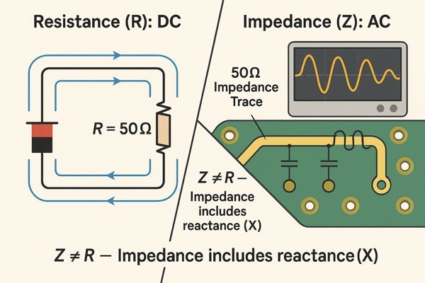
Your simulation shows your driver can handle the load, but on the real PCB, you see reflections and ringing on your high-speed signals. Treating a \(50 \Omega\) trace like a simple resistor is causing signal integrity nightmares. The solution lies in understanding impedance (\(Z\)), the true opposition to AC current, which is far more than just resistance (\(R\)).
Resistance (\(R\)) is the opposition to current flow that is constant regardless of frequency. Impedance (\(Z\)) is the total opposition to AC current, which includes both resistance (\(R\)) and frequency-dependent reactance (\(X\)). The formula is \(Z = R + jX\).
Designing for Transmission Lines
At high frequencies, a PCB trace acts like a transmission line. You must control its characteristic impedance1 to match the driver and receiver. This prevents signal energy from reflecting, which causes ringing and data errors. Impedance is a function of the trace geometry, not just the material. Impedance (\(Z\)) is determined by the physical geometry of the trace—its width (\(w\)), its height (\(h\)) above the reference plane, and the dielectric constant (\(\epsilon_r\)) of the PCB material.
- \(Z = \sqrt{R^2 + (X_L - X_C)^2}\)
- Inductive Reactance (\(X_L\)): \(X_L = 2\pi fL\)
- Capacitive Reactance (\(X_C\)): \(X_C = \frac{1}{2\pi fC}\)
| Property | Symbol | Depends on Frequency? | Key Factors | Impact on High-Speed Signals |
|---|---|---|---|---|
| Resistance | \(R\) | No | Material resistivity, trace length, cross-section. | Contributes to DC loss (\(IR\) Drop). |
| Impedance | \(Z\) | Yes | Trace geometry (\(w\), \(h\)), dielectric constant (\(\epsilon_r\)). | Determines signal reflections and quality. Must be controlled. |
Different high-speed interfaces are designed to work with specific impedance values. Your PCB layout must be designed to meet these targets.
| Interface | Type | Typical Impedance Target |
|---|---|---|
| USB 2.0 | Differential Pair | \(90 \Omega \pm 15\%\) |
| Ethernet (100/1000-BaseT) | Differential Pair | \(100 \Omega \pm 15\%\) |
| DDR3 / DDR4 Memory | Single-Ended | \(40, 50, \text{ or } 60 \Omega\) |
| PCIe | Differential Pair | \(85 \Omega \text{ or } 100 \Omega\) |
| Coaxial (RF) | Single-Ended | \(50 \Omega \text{ or } 75 \Omega\) |
Why does alternating current follow the path of least impedance?
You designed your PCB with a huge, solid ground plane, thinking it would solve all your noise problems. Yet, you're still seeing crosstalk between adjacent high-speed traces. The problem isn't the signal path; it's the invisible return path. This happens because AC return current follows the path of least impedance, not the shortest path.
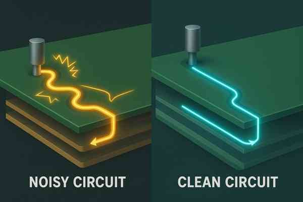
Alternating current follows the path of least impedance. At high frequencies, this impedance is dominated by inductive reactance (\(X_L = 2\pi fL\)). The path with the smallest current loop area creates the lowest inductance, so the return current is forced to flow directly under the signal trace to minimize this loop.
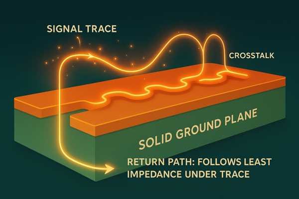
Controlling Crosstalk by Controlling the Return Path
Every signal and its return path form a loop. At high frequencies, the return current constricts itself to flow directly under the signal trace to minimize this loop's area, which minimizes inductance. By ensuring a solid plane beneath our high-speed traces, we force the return current to be tightly coupled. This contains the magnetic field in a small area and dramatically reduces crosstalk2. Following these best practices is not optional for high-speed design.
| Best Practice | Reason / Benefit |
|---|---|
| Maintain a Solid Reference Plane | Provides an unbroken, low-inductance path for the return current to flow directly under the signal trace. |
| Route Over Planes, Not Traces | Routing a high-speed signal over a power trace instead of a solid plane creates a very poor, high-inductance return path. |
| Use Stitching Vias at Plane Transitions | When a signal changes layers, a nearby "stitching" via gives the return current a short path to follow the signal to the new reference plane. |
| Avoid Crossing Gaps/Splits | Forcing the return current around a gap creates a large loop, which increases inductance and EMI, and destroys signal integrity. |
How does frequency affect the path of a return current?
A mixed-signal design is failing because digital noise is getting into your sensitive analog section. You carefully isolated the grounds with a "moat" between them, but this common practice is actually making the noise worse. Understanding how the return path changes with frequency reveals why a single, well-designed ground plane is often superior.
At low frequencies, the return current takes the path of least resistance (the shortest path). At high frequencies, it switches to the path of least inductance (directly under the signal trace). The "crossover point" where inductance starts to dominate is typically in the \(50 \text{ kHz}\) to \(100 \text{ kHz}\) range.
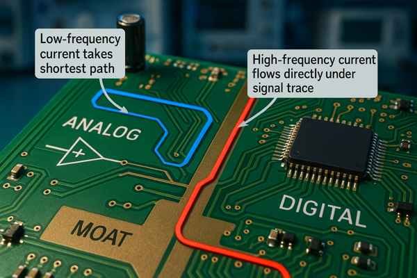
Why Split Grounds Are Often a Bad Idea
The classic "split plane" approach for mixed-signal boards is now largely considered outdated for most designs. If any signal trace must cross the split, its high-frequency return current is forced on a long detour, creating a massive antenna that couples noise between the sections. A much better modern strategy is to use a single, solid ground plane and practice intelligent component placement.
| Grounding Strategy | How It Works | Pros | Cons / Risks |
|---|---|---|---|
| Split Ground Plane3 | Separate AGND and DGND planes, connected at one point (star ground). | Simple concept. Can work for low-frequency circuits with no crossing signals. | Creates a "slot antenna" if any trace crosses the split. High risk of severe EMI and noise coupling. |
| Solid Plane w/ Partitioning | One continuous ground plane. Digital and analog components are placed in separate areas (partitions). | Provides the lowest impedance return path for all signals. Prevents return path loops. | Requires careful layout planning to keep noisy digital return currents away from sensitive analog areas. |
This table below summarizes the entire journey of the return current as frequency changes.
| Frequency Range | Dominant Factor | Return Current Behavior | Consequence of Poor Design |
|---|---|---|---|
| DC to \(\approx 10 \text{ kHz}\) | Resistance (\(R\)) | Spreads across the plane, follows the shortest path. | Excessive \(IR\) drop, causing voltage sag and component malfunction. |
| \(\approx 50 \text{ kHz}\) to \(1 \text{ MHz}\) | Transition | A mix of resistance and inductance control the path. | Unpredictable behavior; can be a source of hard-to-diagnose noise. |
| \(>1 \text{ MHz}\) | Inductance (\(L\)) | Tightly coupled directly underneath the signal trace. | Signal reflections4, ringing, crosstalk, and radiated emissions failures. |
Conclusion
From minimizing DC voltage drop to providing a tightly coupled path for high-frequency signals, mastering the return current is non-negotiable. It's the key to passing EMC and building robust, reliable hardware that works every time.
-
Understanding characteristic impedance is crucial for designing effective transmission lines and preventing signal issues. ↩
-
Explore various techniques to minimize crosstalk, ensuring better performance in your high-speed electronic designs. ↩
-
Understanding the drawbacks of split ground planes can help you make better design choices for mixed-signal circuits. ↩
-
Signal reflections can severely impact circuit performance. Discover how to mitigate these issues for better reliability in your designs. ↩


