 Skip to content
Your board suffers from random, maddening glitches that defy simulation. These intermittent failures are a nightmare to debug, wasting your time and budget. The problem is likely a bad return path.
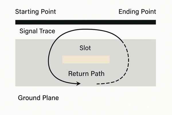
A return path discontinuity occurs when the path for the return current, typically on a ground plane, is obstructed by a gap, slot, or change in reference plane. This forces the current to find a longer route, which increases the loop inductance, creating signal integrity degradation, noise, and severe EMI problems.
As a hardware engineer for nearly 20 years, I've seen countless projects get derailed by problems that were incredibly hard to debug. More often than not, the root cause wasn't a faulty component or a complex software bug. It was something much more fundamental that was missed during layout: a poorly designed return path. I learned this lesson the hard way on expensive, high-stakes projects. An oversight that looks tiny on a layout screen can become a massive failure in the EMC test chamber. Let's break down why this path is so critical and how to keep it clean so you don't repeat the same costly mistakes.
What is a "current loop" in a PCB and why is it bad?
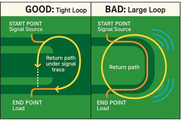
Your design is unexpectedly failing EMI testing despite a solid ground plane (P). Now you face costly lab fees and frustrating project delays, a major setback (A). The culprit is likely an unseen "current loop."
A "current loop" is the complete path a signal takes from the source to the load and back. When the return path is forced away from the signal trace, it creates a larger loop area. Physics dictates that this large loop acts as an efficient antenna, radiating electromagnetic energy (EMI) and making your device fail compliance tests.
The Physics of the Path of Least Impedance
At DC or very low frequencies, current takes the path of least resistance. But as signal frequencies climb into the megahertz range and beyond, physics changes the rules. The current now takes the path of least impedance, which is dominated by inductance. To minimize inductance, the return current wants to flow in the path that creates the smallest possible loop area. This means it naturally tries to flow directly underneath the signal trace in the adjacent ground or power plane. This close coupling cancels out the magnetic fields, containing the energy and preventing it from radiating.
When you introduce a discontinuity—like a slot for a component, a cutout, or routing a trace over a split between analog and digital grounds—you break this ideal, low-inductance path. The return current is now forced to detour, like a river flowing around a dam. This detour dramatically increases the area of the current loop. The amount of radiated energy is directly proportional to this loop area and the square of the frequency. A larger loop acts as a more efficient antenna, broadcasting noise.
During the Tuxedo Keypad project at Honeywell, we faced an unexpected EMI failure. The device was radiating too much noise around the Wi-Fi module's frequency band. We spent days in the lab trying to shield the module, but nothing worked. We finally traced the problem to a set of control lines that crossed a small, \(3 \text{ mm}\) gap in the ground plane near a connector. The return current had to travel \(4 \text{ cm}\) around this gap, creating a large loop that was a perfect antenna. The fix, which required a board spin, was to add a single \(10 \text{ nF}\) 0402 ceramic capacitor to "stitch" the ground planes together right where the traces crossed. This gave the high-frequency return current a local, low-impedance bridge. The change reduced the radiated peak by \(12 \text{ dB}\), pushing us comfortably below the CISPR limit and saving the schedule.
| Feature | Small Loop Area (Good) | Large Loop Area (Bad) |
|---|---|---|
| Return Path | Directly under signal trace | Long detour around an obstacle |
| Loop Inductance | Low (e.g., \(<1 \text{ nH}\)) | High (e.g., \(>10 \text{ nH}\)) |
| EMI Radiation | Minimal | Significant |
| Signal Quality | High | Degraded (Ringing, Overshoot) |
How does a poor return path cause electromagnetic interference (EMI)?
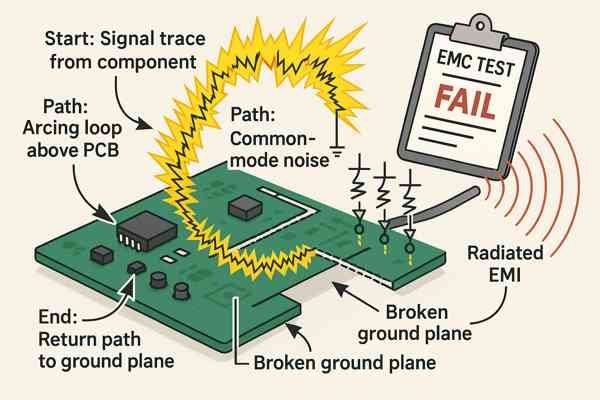
Your product just failed its EMC test because of radiating cables (P). This failure can halt your product launch and trigger a costly, urgent redesign (A). It's all caused by a poor return path.
A poor return path creates a large current loop. This loop forces a voltage difference between different "ground" points on the board, creating common-mode noise. This noise then finds its way onto external cables, which act as highly efficient antennas, radiating EMI and causing compliance failures.
How Cables Become Unintentional Transmitters
The most difficult EMI to control is common-mode radiation. A return path discontinuity is a primary generator of this noise. When a high-speed signal's return current has to detour, it flows through a path with higher impedance. This creates a voltage drop across the return path. As a result, the ground potential at the driver IC is now different from the ground potential at the receiver IC or the chassis ground connection. This voltage difference is common-mode voltage1, and it will drive a current down any conductive path it can find—most notably, the shields and conductors of I/O cables (USB, Ethernet, power).
Cables are the worst offenders because their length makes them incredibly efficient antennas at typical electronic device frequencies (\(30 \text{ MHz} - 1 \text{ GHz}\)). As frequency increases, a simple wire's impedance rises, making it a better antenna. According to EMC experts like Dr. Clayton R. Paul, it takes astonishingly little common-mode current to fail regulatory tests. For a product to meet CISPR 32 / FCC Part 15 Class B2 limits, the maximum allowable common-mode current on an external cable is often in the range of 5 to 50 microamps (\(\mu A\)).
The table below shows why a typical 1-meter cable is so effective at radiating noise. Its impedance increases with frequency, turning it from a simple wire into an efficient antenna precisely in the frequency range where most radiated emissions tests are performed.
| Frequency | Wavelength (\(\lambda\)) | Electrical Length (for 1m cable) | Typical Common-Mode Impedance |
|---|---|---|---|
| \(10 \text{ MHz}\) | \(30 \text{ m}\) | \(\frac{\lambda}{30}\) | Low (\(\approx 50 \Omega\)) |
| \(30 \text{ MHz}\) | \(10 \text{ m}\) | \(\frac{\lambda}{10}\) | Moderate (\(\approx 100 \Omega\)) |
| \(100 \text{ MHz}\) | \(3 \text{ m}\) | \(\frac{\lambda}{3}\) | High (\(\approx 250 \Omega\)) |
| \(300 \text{ MHz}\) | \(1 \text{ m}\) | \(\frac{\lambda}{1}\) | Very High (\(\approx 400 \Omega\)) |
This is why proper grounding of connectors and ensuring a solid ground plane underneath all high-speed traces right up to the connector pins is non-negotiable for passing EMI tests.
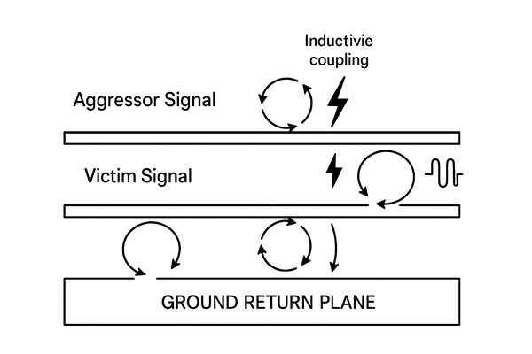
Your signals are corrupting each other, creating random data errors (P). This crosstalk leads to unreliable performance and frustrating debugging sessions (A). The cause is often the shared return current, not trace spacing.
Crosstalk is the unwanted transfer of energy from one signal trace (the aggressor) to a nearby trace (the victim). While capacitive coupling between traces is a factor, a compromised or shared return path creates strong inductive coupling. The magnetic field from the aggressor's return current induces a noise voltage in the victim's loop.
The Hidden Role of Mutual Inductance
Engineers often use the "3W rule" (keep traces separated by at least three times their width) to manage crosstalk. This rule is a decent starting point, but it's only effective because it assumes a solid, continuous ground plane directly below the traces. This ideal plane ensures the return current for each signal stays tightly confined under its respective trace, minimizing the interaction of their magnetic fields.
When the return path is compromised—for instance, on a board with a heavily perforated ground plane or no ground plane at all—the return currents spread out and are forced to share copper. This sharing creates mutual inductance3. Just as two coils in a transformer are linked by a magnetic field, the two signal loops are now linked by their shared return path. They have become a tiny, unwanted transformer. The rapidly changing current in the aggressor loop (\(\frac{di}{dt}\)) induces a noise voltage in the victim loop, corrupting its signal.
The table below shows how different layout strategies impact crosstalk. Notice how a good return path is more critical than spacing alone.
| Layout Strategy | Description | Return Path Quality | Expected Crosstalk Level |
|---|---|---|---|
| 2W Spacing, No Plane | Traces are routed close together with no ground plane. | Very Poor (Trace Return) | Very High |
| 3W Spacing, Split Plane | Traces adhere to 3W but cross a ground plane split. | Poor | High |
| 3W Spacing, Solid Plane | The standard "best practice" implementation. | Good | Low |
| Guard Trace, Solid Plane | A grounded trace is placed between aggressor and victim. | Excellent | Very Low |
A common mistake I see is the use of a "guard trace" that isn't properly grounded. For it to work, it must be connected to the ground plane with vias at regular intervals (e.g., every \(5-10 \text{ mm}\)). These vias provide a low-inductance path for the coupled noise, shunting it to ground. A floating guard trace is useless and can sometimes make things worse.
What Is ground bounce and what causes It?
Your processor resets randomly even with a clean power supply (P). These phantom bugs can make your entire system unstable and untrustworthy (A). You are likely experiencing "ground bounce."
Ground bounce, or Simultaneous Switching Noise (SSN), is a transient voltage spike on the ground rail. It's caused by a large, rapid change in current (\(\frac{di}{dt}\)) from many outputs switching at once, flowing through the inherent inductance (\(L\)) of the IC package and PCB ground path. This creates a voltage spike according to the law of inductance, \(V = L \cdot \frac{di}{dt}\).
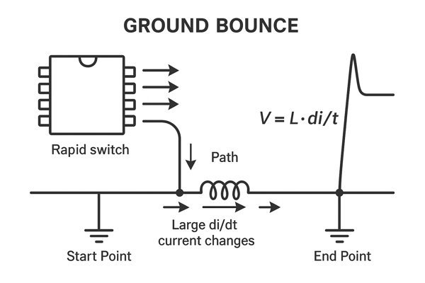
Ground Bounce Suppression Techniques: An Example
The formula \(V = L \cdot \frac{di}{dt}\) is simple but has profound implications. The \(L\) is the total inductance from the silicon die, through the package lead frame or BGA ball, through the PCB via, and into the ground plane. The \(\frac{di}{dt}\) is the rate of change of current, which is massive when multiple outputs switch simultaneously.
Let's run a detailed scenario. An FPGA is driving 16 outputs low at the same time.
- Package and via inductance (\(L\)) per pin: \(4 \text{ nH}\) (a realistic value for a standard QFP package).
- Current sink (\(I\)) per pin: \(8 \text{ mA}\).
- Signal fall time (\(dt\)): 500 picoseconds (\(ps\)).
The total \(\frac{di}{dt}\) is \(\frac{(16 \text{ pins} \times 8 \text{ mA})}{500 \text{ ps}} = \frac{128 \text{ mA}}{500 \text{ ps}} = 256 \times 10^9 \text{ A/s}\).
The ground bounce voltage (\(V\)) is:
\(V = 4 \text{ nH} \times (256 \times 10^9 \text{ A/s}) = 1.024 \text{ V}\)
A full \(1\text{-volt}\) bounce on your "solid" 0V ground reference is a disaster! To combat this, we use decoupling capacitors. The key is to choose capacitors that are effective at the frequencies of interest. A capacitor's effectiveness is limited by its Equivalent Series Inductance (ESL) and its Self-Resonant Frequency (SRF). You need caps that have low impedance at your noise frequencies.
| Capacitor Value | Typical Package | Approx. ESL | Approx. SRF | Best For Suppressing... |
|---|---|---|---|---|
| \(1.0 \mu\text{F}\) | 0603 | \(700 \text{ pH}\) | \(\approx 15 \text{ MHz}\) | Lower frequency bulk noise |
| \(100 \text{ nF}\) | 0402 | \(500 \text{ pH}\) | \(\approx 50 \text{ MHz}\) | Mid-frequency core noise |
| \(10 \text{ nF}\) | 0402 | \(450 \text{ pH}\) | \(\approx 160 \text{ MHz}\) | High-frequency I/O noise |
| \(1 \text{ nF}\) | 0201 | \(300 \text{ pH}\) | \(\approx 500 \text{ MHz}\) | Very high-frequency noise |
Placing a bank of these capacitors (e.g., \(10 \text{ nF}\), \(100 \text{ nF}\)) right next to each power/ground pin pair provides a local charge reservoir to service the high \(\frac{di}{dt}\) demand, minimizing the voltage drop across the package inductance.
Conclusion
A clean, continuous return path is not just a "best practice"; it is an absolute requirement for modern electronics. It’s the fundamental building block of a stable, reliable, and compliant design, preventing EMI, crosstalk, and ground bounce before they start.
-
Understanding common-mode voltage is crucial for managing EMI in electronic devices, ensuring compliance with regulatory standards. ↩
-
Exploring these standards helps manufacturers ensure their products meet necessary compliance for electromagnetic interference. ↩
-
Understanding mutual inductance is crucial for engineers to design circuits that minimize noise and improve signal integrity. ↩


