 Skip to content
Are your high-speed differential signals failing, even though the design looks correct? You've followed the rules, but intermittent errors and EMI failures are causing major headaches and project delays.
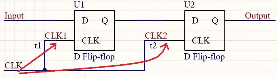
Skew is a timing mismatch between two or more related signals. In a differential pair, it’s the time difference between when the positive (\(P\)) and negative (\(N\)) signals arrive at the receiver. This mismatch is a primary cause of signal integrity degradation and EMI.
As a hardware engineer for nearly 20 years, I've seen countless projects get derailed by problems that could have been prevented at the layout stage. Skew is one of those silent killers. It's a simple concept, but its effects are profound, turning a perfectly designed circuit into a source of failure. Understanding and controlling skew is not just a "best practice"—it's a fundamental requirement for modern electronics. Let's break down what skew really is, where it comes from, and how you can manage it effectively in your own designs.
What is the Difference Between Skew and Jitter?
Confusing the terms skew and jitter is a common mistake. This can lead you down the wrong path during debugging, wasting valuable time chasing a noise issue when the real problem is a layout flaw.
Skew is a static, repeatable timing difference between two different signals caused by path length mismatches. Jitter is a dynamic, non-repeatable timing variation of a single signal edge relative to its ideal position over time, often caused by noise.
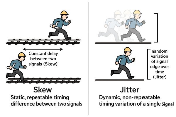
To properly diagnose issues, you have to understand this core difference. In my experience leading hardware development, we had to hunt down both. On a complex data acquisition system, we saw consistent errors on a parallel bus which pointed to a timing relationship problem between signals. That was skew. On a separate project, a high-speed serial link was unstable, and measurements showed the clock edges were shifting randomly. That was jitter. They are two different problems requiring different solutions.
Defining Skew as a Spatial Mismatch Between Signals
Think of skew as a problem of space or path. Imagine two runners who are supposed to start and finish a race at the exact same time. If one runner is assigned a track that is 10 meters longer, they will always finish after the other runner by a predictable amount of time. This fixed time difference is skew. In a PCB, the "track" is the copper trace, and the "runner" is the electrical signal. A longer trace means a longer travel time. Skew is deterministic because it's baked into the physical design.
Defining Jitter as a Temporal Variation on a Single Signal
Jitter, on the other hand, is a problem of time. It's not a fixed offset, but a variation on a single signal. Jitter itself has two main components:
- Random Jitter1 (\(RJ\)): This is unbounded, Gaussian noise caused by thermal effects and other random physical processes. You can't predict it, only characterize it statistically (e.g., as an RMS value).
- Deterministic Jitter2 (\(DJ\)): This is bounded and repeatable. It's caused by predictable sources like crosstalk from a neighboring signal or periodic noise from a switching power supply.
Expert Insight: How Skew Fits into the Overall Jitter Budget
Here is where the concepts merge at an expert level. The total timing uncertainty at a receiver is called the Total Jitter3 (\(TJ\)), often specified for a target Bit Error Rate (e.g., \(10^{-12}\)). The \(TJ\) is a statistical sum of \(RJ\) and \(DJ\): \(TJ = N \times RJ_{RMS} + DJ_{pk-pk}\).
Intra-pair skew contributes directly to the Deterministic Jitter budget. Specifically, it creates a form of Inter-Symbol Interference (\(ISI\))4, as the misaligned \(P\) and \(N\) edges distort the final differential waveform. When you build a jitter budget for a SerDes link, the margin allocated for \(ISI\) must account for the effects of skew. It's not a separate phenomenon; it's a direct contributor to the total jitter that closes the eye.
What Are the Two Types of Differential Skew (Intra-pair and Inter-pair)?
Knowing that skew exists isn't enough. In any system with more than one differential pair, you are dealing with two distinct types of skew, and a failure to manage both can lead to system failure.
Intra-pair skew is the timing mismatch between the \(P\) and \(N\) traces within a single differential pair. Inter-pair skew is the a timing mismatch between two or more different differential pairs, such as a clock pair and a data pair.
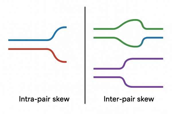
The table below provides a clear comparison between these two critical concepts.
| Feature | Intra-Pair Skew | Inter-Pair Skew |
|---|---|---|
| Definition | Timing mismatch between the \(P\) and \(N\) traces of a single pair. | Timing mismatch between multiple pairs in a group (e.g., clock vs. data). |
| Primary Effect | Converts differential signal to common-mode noise, causing EMI. | Causes data sampling errors at the receiver. |
| Typical Tolerance | Very tight (e.g., \(< 1 \text{ ps}\) for \(10 \text{ Gbps}\) signals). | Looser, but still critical (e.g., \(< 100 \text{ ps}\) for DDR4). |
| Governed By | Physics of field cancellation and signal integrity. | System timing budget and interface protocol specification. |
| Example | Length matching the \(P\) and \(N\) traces of a single USB 3.0 pair. | Length matching all 8 \(DQ\) pairs to the \(DQS\) pair in a DDR4 byte lane. |
Expert Insight: The Trade-offs of Using Serpentine Length Tuners
Your EDA software is your primary weapon against skew. You create matched-length constraints and the tool adds serpentine structures to the shorter traces. However, an experienced designer knows these tuners are a necessary evil.
- Impedance Discontinuity: The bends in the serpentine have a different impedance than the straight sections. While modern tools use arcs to minimize this, it's not perfect.
- Increased Crosstalk: The segments of the serpentine are now running parallel to each other in close proximity. This "broadside coupling" increases crosstalk and can degrade the signal you're trying to fix.
- Mode Conversion: The asymmetry of the bends can introduce its own mode conversion.
For ultra-high-speed designs (56+ Gbps PAM4), best practice is to minimize or even eliminate serpentine tuners. This requires meticulous floorplanning and "routing studies" early in the design process to ensure signal paths are naturally of similar length. This is a key difference between a journeyman and an expert layout engineer.
What Are the Primary Causes of Skew in a PCB Layout?
You've spent weeks on schematic design, but it can all be undone by a few poor choices in the layout phase. Skew doesn't happen by accident; it is introduced by specific, and often avoidable, layout practices.
The primary causes of skew in a PCB layout are unequal physical trace lengths, routing the \(P\) and \(N\) traces on different layers with different propagation speeds, the fiber weave effect in the PCB substrate, and asymmetries in component pads or via usage.
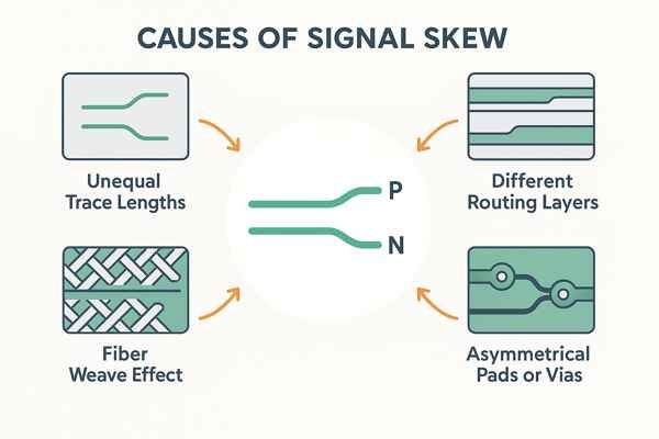
The following table summarizes these common causes and, more importantly, the primary strategies to prevent them.
| Cause of Skew | Description | Primary Mitigation Strategy |
|---|---|---|
| 1. Unequal Trace Lengths | The \(P\) and \(N\) traces have different physical lengths. | Use EDA tool's length-tuning features (serpentine traces) to add length to the shorter trace. |
| 2. Layer Speed Mismatch | \(P\) and \(N\) traces are routed on different layers (e.g., microstrip vs. stripline). | Keep \(P\) and \(N\) traces on the same layer for their entire routed length. |
| 3. Fiber Weave Effect | Non-uniform dielectric constant in the PCB material (FR-4). | Route at an angle (e.g., \(10^{\circ}\)) or specify uniform-weave materials (e.g., spread-glass). |
| 4. Asymmetrical Vias & Stubs | One trace uses a via while the other doesn't, or via stubs are present. | Maintain symmetry; if one trace has a via, add one to the other. Use back-drilling for stubs. |
| 5. Asymmetric Driver Rise/Fall | The driver IC produces different rise and fall times. | Select high-quality ICs; simulate driver-channel co-design. Cannot be fixed in layout alone. |
Cause 4: Asymmetrical Vias and Via Stubs (In Depth)
Vias are a major source of skew. A through-hole via that passes from layer 1 to layer 2 on a 12-layer board leaves a long, unused barrel from layer 2 to layer 12. This "via stub" acts as a resonant antenna. The first resonant frequency of the stub can be approximated by: \(f_{res} \approx \frac{c}{4 \times L_{stub} \times \sqrt{\epsilon_{r}}}\) where \(c\) is the speed of light, and \(L_{stub}\) is the stub length. If this frequency falls within the bandwidth of your signal, it will cause severe reflections and \(ISI\).
- Mitigation 1 (Symmetry): If one trace needs a via, add one to the other trace as well, to balance the delays.
- Mitigation 2 (Back-drilling): For critical signals, use back-drilling (Controlled Depth Drilling) to remove the unused stub. This adds cost but is often mandatory for 25+ Gbps links.
How Does Skew Affect Common-Mode Rejection in a Differential Pair?
You chose to use a differential pair specifically for its excellent noise immunity (Common-Mode Rejection Ratio, or \(CMRR\)). But introducing skew can completely undermine this core advantage, making your circuit vulnerable to noise.
Skew causes the \(P\) and \(N\) signals to arrive at the receiver at different times. This prevents the common-mode noise present on both lines from being perfectly cancelled out by the differential receiver, effectively degrading the system's \(CMRR\).
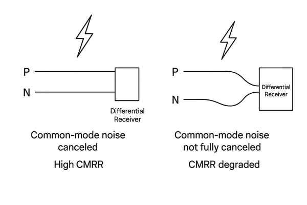
The Ideal Differential Pair: How Common-Mode Noise is Cancelled
A differential receiver subtracts its inputs: \(V_{diff} = V_{P} - V_{N}\). If common-mode noise, \(V_{cm}\), is added to both lines, the receiver sees \((V_{P} + V_{cm}) - (V_{N} + V_{cm}) = V_{P} - V_{N}\). The noise, \(V_{cm}\), is perfectly cancelled.
The Skewed Pair: Why Noise Cancellation Fails
With skew, the \(N\) signal is delayed by \(t_{skew}\). The receiver performs this subtraction: \(V_{out}(t) = (V_{P}(t) + V_{cm}(t)) - (V_{N}(t+t_{skew}) + V_{cm}(t+t_{skew}))\). Because the noise terms \(V_{cm}(t)\) and \(V_{cm}(t+t_{skew})\) are no longer aligned, they don't subtract to zero.
Expert Insight: Modeling Mode Conversion with S-Parameters (Scd21)
This conversion of energy from differential mode to common mode is a critical concept. In the frequency domain, it is characterized by S-parameters5. Specifically, the parameter \(S_{cd21}\) (or sometimes \(S_{DC21}\)) represents the transfer function from a differential input (port 1) to a common-mode output (port 2). An ideal, perfectly symmetrical pair would have an \(S_{cd21}\) of negative infinity (zero conversion). Any skew in the physical channel will cause the \(S_{cd21}\) value to rise at higher frequencies, providing a direct, quantifiable measure of how much mode conversion the channel will produce. When we evaluated prototype boards at Lightelligence, analyzing the \(S_{cd21}\) from VNA measurements was a key step in validating the layout.
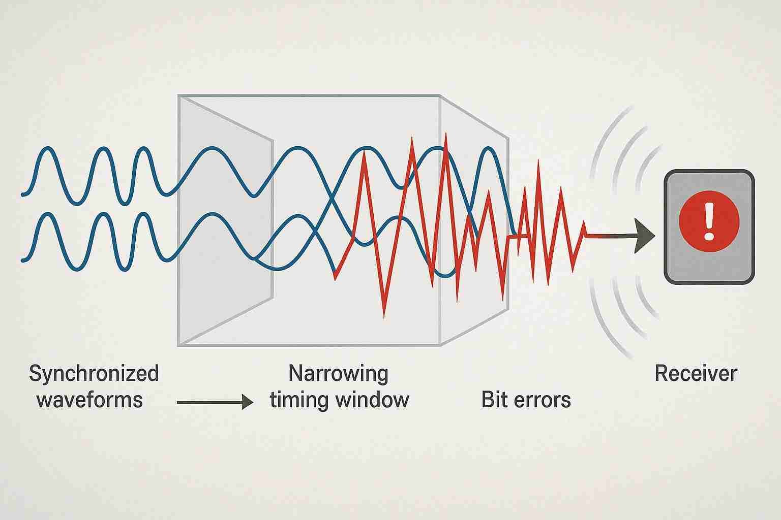
What Are the Effects of Excessive Skew on a High-Speed Signal?
A little bit of skew might be unavoidable, but how much is too much? Pushing the limits of your timing budget with excessive skew can lead to a range of problems, from intermittent glitches to complete system failure.
Excessive skew directly reduces the valid data window (timing margin), increases the Bit Error Rate (\(BER\)), generates significant electromagnetic interference (\(EMI\)) due to common-mode conversion, and ultimately leads to link failure when it exceeds the receiver's tolerance.
This table summarizes the cascading consequences of uncontrolled skew.
| Effect of Skew | Impact Domain | Key Metric Degraded |
|---|---|---|
| Reduced Timing Margin | Signal Integrity | Usable Unit Interval (\(UI\)), Eye Width |
| Increased Bit Error Rate (\(BER\)) | System Performance | Link stability, Data throughput |
| EMI Generation | Product Compliance | Radiated & Conducted Emissions (FCC/CE) |
| Impaired Equalization | Advanced SI / System | Receiver's \(DFE\)/\(CTLE\) effectiveness |
Effect 4: Impairment of the Receiver's Equalization Circuitry
This is a critical second-order effect that many engineers overlook. Modern SerDes receivers (in FPGAs, ASICs) use powerful digital equalizers like Continuous Time Linear Equalization (\(CTLE\))6 and Decision Feedback Equalization (\(DFE\))7 to compensate for frequency-dependent channel loss. These equalizers are designed and trained to correct for impairments in the differential signal path. However, significant skew introduces common-mode noise and non-linear distortions that these equalization circuits are not designed to handle. Excessive skew can confuse the \(DFE\)'s adaptation algorithm, causing it to apply the wrong correction and actually increase the \(BER\). In essence, skew can poison the very mechanism designed to save the signal.
How Does Skew Convert Differential Signals into Common-Mode Noise?
You designed a differential pair to be electromagnetically "quiet" by containing its fields. So why is it suddenly failing EMC testing and radiating noise like an antenna? The answer often lies in how skew breaks this fundamental principle.
Skew creates a time mismatch between the equal and opposite currents in the \(P\) and \(N\) traces. This imbalance prevents their magnetic fields from canceling each other out perfectly, resulting in a net "common-mode" current that radiates electromagnetic energy.
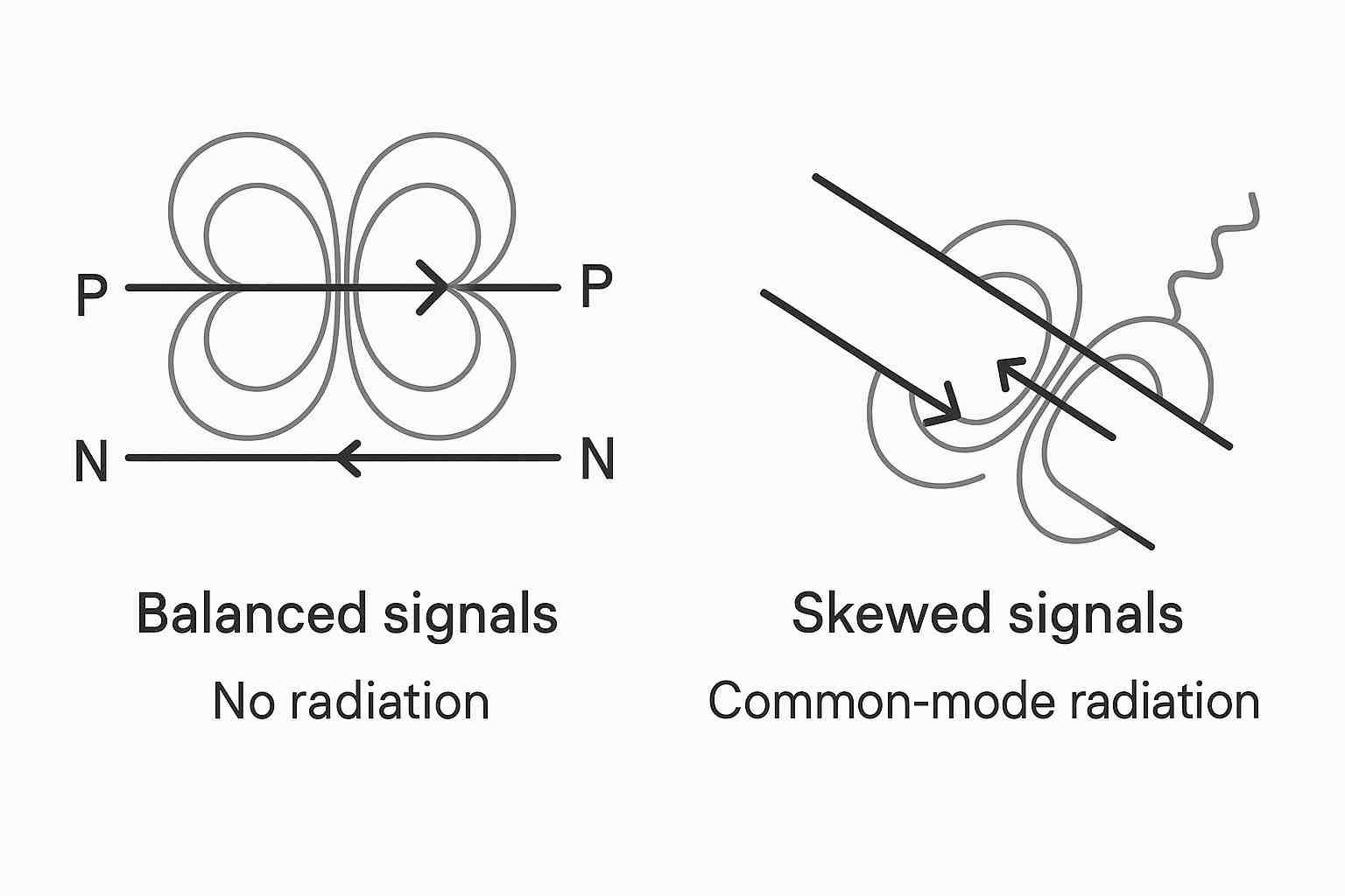
The Ideal Differential Pair: How Magnetic Fields are Cancelled
In an ideal pair, the current \(I_{P}\) flows out, and the equal, opposite current \(I_{N}\) flows back. The loop for this differential current is extremely small—just the area between the \(P\) and \(N\) traces. Because the loop area is tiny and the fields are opposing, very little energy escapes.
The Skewed Pair: Creation of the Common-Mode Current Loop
With skew, the currents become unbalanced, creating a common-mode current8, \(I_{cm}\). This current flows in the same direction on both traces. To complete its circuit, it must find a return path, which is typically the nearest solid reference plane (e.g., ground).
The Result of Skew: A Large, Efficient Radiating Antenna
The loop for this new common-mode current is the area between the differential pair and its reference plane. This loop is orders of magnitude larger than the differential mode loop. The efficiency of an unintentional loop antenna is directly proportional to its area. Because the common-mode loop is so large, it becomes a very efficient antenna, broadcasting noise at the signal's fundamental frequency and its harmonics. This is the physical mechanism behind EMI failures caused by skew.
How Does Skew Impact the Eye Diagram of a Signal?
The eye diagram is one of the most powerful tools for visualizing the health of a high-speed signal. If your eye diagram looks sick—small, blurry, or closed—skew could be the culprit, and it leaves a very specific signature.
Intra-pair skew causes the rising and falling edges of the differential signal to have different apparent slew rates. This appears on an oscilloscope's eye diagram as a split or "thickening" of the crossover point, reducing both the height (voltage margin) and width (timing margin) of the eye.
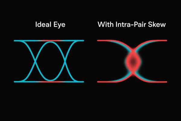
Visualizing a Healthy Signal with an Open Eye Diagram
When I'm debugging a link, the eye diagram is my first stop. A healthy signal produces a wide-open eye. The lines are thin, the transitions cross at a single, clean point in the middle (the crossover point), and the opening is tall and wide. This indicates plenty of timing and voltage margin.
Identifying Skew's Signature: The Split Crossover Point
Intra-pair skew causes a distinct artifact. The differential signal is \(V_{P} - V_{N}\). If one is delayed, the resulting edge is distorted. This makes the rising and falling edges in the eye diagram no longer cross at the same voltage level. Instead of one sharp crossover point, you see two, or a blurred horizontal region where the crossover should be.
Expert Insight: Advanced Skew Measurement and De-embedding Techniques
While the split crossover is a classic sign, in a real-world system, it's often obscured by other impairments like random jitter and \(ISI\). This is where advanced tools become invaluable.
- Jitter Decomposition: Modern real-time oscilloscopes have software that can decompose the total jitter into its components (\(RJ\), \(DJ\), \(ISI\), etc.). The portion of \(DJ\) that correlates with the data pattern can often be traced back to skew and other \(ISI\) sources.
- Skew Measurement: Some oscilloscopes offer a direct
T-skewmeasurement that attempts to calculate the time difference between the \(P\) and \(N\) zero-crossings, giving a quantitative value for the skew that is causing the eye distortion. - De-embedding: The ultimate analysis involves measuring the channel's S-parameters with a Vector Network Analyzer (VNA) and using software (like MATLAB or Keysight's ADS) to create a model of the channel. This allows you to simulate the link's performance and mathematically "de-embed" the effects of the cables and test fixtures, isolating the skew that is present on the DUT itself. This is the gold standard for root cause analysis in high-stakes projects.
Conclusion
Skew is not a trivial detail; it's a fundamental parameter in high-speed design. It is a deterministic flaw introduced during layout that reduces margins, creates noise, impairs receiver performance, and causes system failures. Mastering it is essential.
-
Learn how random jitter impacts signal quality and why understanding its sources is crucial for reliable high-speed circuit design. ↩
-
Learning about Deterministic Jitter provides insights into predictable timing variations, essential for effective circuit design. ↩
-
Understanding Total Jitter is key for engineers to manage timing uncertainties and improve system reliability. ↩
-
Learn how Inter-Symbol Interference (ISI) affects signal integrity and why managing ISI is crucial for reliable high-speed data transmission. ↩
-
Exploring S-parameters will enhance your knowledge of signal transmission and help in designing better electronic circuits. ↩
-
Learn how CTLE improves signal integrity in high-speed data links and why it's crucial for compensating channel loss in modern electronic systems. ↩
-
Learn how DFE technology improves signal integrity in high-speed data links and why it's crucial for reliable communication in modern electronics. ↩
-
Understanding common-mode current is crucial for designing circuits that minimize noise and improve performance. ↩


