 Skip to content
Struggling with signal integrity or EMI issues in your designs? Your PCB stackup might be the hidden culprit, often overlooked yet critically important.
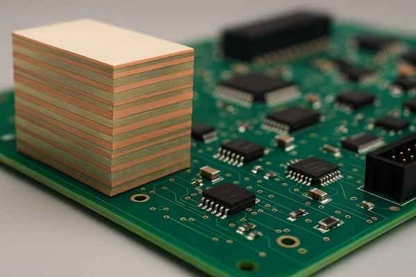
A PCB stackup is the arrangement of copper layers and insulating materials that make up a printed circuit board. It dictates crucial electrical properties like impedance, crosstalk, and EMI performance, which are essential for modern electronics.
Now that we know what a PCB stackup is and why it's so important, you might have more specific questions about its construction and the materials involved. Let's dive into those details to give you a clearer picture of how these layers come together to make your electronics work effectively, because understanding these nuances is key to successful hardware design.
Why do PCBs have layers?
Ever wondered why simple circuits become complex multi-layered boards? It’s not just about fitting more components into a smaller space.
PCBs have multiple layers to route complex circuits, manage signal integrity effectively, provide stable power and ground planes, and shield sensitive signals. This layering allows for denser, higher-performance, and more reliable designs.
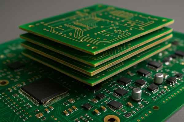
In my nearly 20 years as an embedded systems engineer, I've seen firsthand how moving from a 2-layer to a 4-layer or even an 8+ layer board can be the difference between a product that barely functions and one that performs exceptionally. Here's a deeper look:
Benefits of Multi-Layer PCBs
| Feature | Benefit | My Experience Example |
|---|---|---|
| Signal Routing Density | Accommodates complex circuits with many interconnects by providing multiple routing surfaces. | An industrial controller project required a shift from 2 to 4 layers due to routing impossibilities. |
| Signal Integrity1 | Dedicated ground/power planes offer stable references, reduce return path inductance, and minimize crosstalk. | Essential for high-speed digital designs; a ground plane can cut crosstalk by greater than 20 dB (Source: Johnson & Graham). |
| EMI/EMC Control2 | Internal planes shield signals, reducing emissions and improving immunity to external noise. | Critical for passing compliance tests (FCC, CE) for products like the Tuxedo Keypad. |
| Power Integrity3 | Power planes ensure even power distribution with lower impedance, minimizing voltage drops and noise. | Crucial for sensitive analog circuits and power-hungry digital ICs in medical devices. |
| Component Density | Allows for more components in a smaller footprint by utilizing internal layers for routing, freeing up surface area. | Key for miniaturization in handheld devices like the infusion pump I designed. |
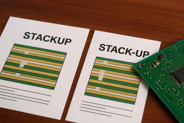
Is a PCB stack-up or Stackup?
Does a tiny hyphen in a technical term really make a difference? When it comes to "stack-up" versus "stackup," consistency is helpful for clarity.
Both "stack-up" (hyphenated) and "stackup" (one word) are commonly used and widely understood in the PCB industry. The single-word "stackup" is becoming more prevalent, especially in technical documentation and software interfaces.
In my experience, the specific form used often comes down to style guides or regional preferences, but the technical meaning remains identical.
Usage Comparison: "Stack-up" vs. "Stackup"
| Aspect | "Stack-up" (Hyphenated) | "Stackup" (One Word) | My Recommendation |
|---|---|---|---|
| Common Usage | Traditional, still found in some standards | Increasingly common, especially in new software | Either is fine if used consistently. |
| Trend | Less prevalent in modern technical writing | Growing in popularity, follows closed-compound trend | Lean towards "stackup" for new documentation. |
| Clarity | Clear | Clear | Consistency is more important than the form. |
| Examples | IPC-2221B sometimes uses "layer stack-up" | Altium Designer uses "Layer Stack Manager" | Check your company's style guide if one exists. |
The most critical aspect isn't which form you choose, but that you use it consistently within your own project documentation, team communications, and when dealing with manufacturers. Clear communication of the technical details of the layer arrangement itself is paramount.
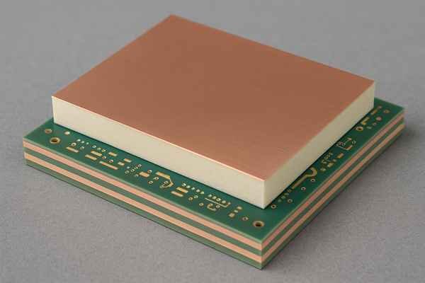
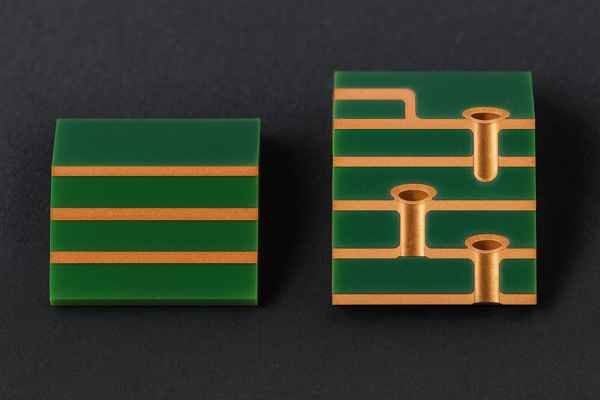
What is the difference between prepreg and core?
Building a multi-layer PCB is like making a high-tech lasagna. Understanding the "ingredients," such as prepreg and core, is vital for any hardware engineer.
In a PCB stackup, a core is a rigid piece of dielectric material (like FR-4) with copper foil already bonded to one or both sides. Prepreg is a pliable, uncured sheet of fiberglass impregnated with resin, used to bond cores and copper foils together during lamination.
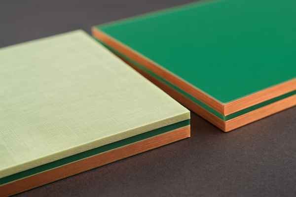
Think of the core as a ready-made, sturdy slice of bread with butter already on it, and prepreg as the cheese that melts and glues multiple slices together.
Core vs. Prepreg: Key Differences
| Feature | Core Material | Prepreg Material |
|---|---|---|
| State | Fully cured (C-stage) dielectric | Partially cured (B-stage) resin system |
| Structure | Rigid sheet, copper-clad on one or both sides by laminate supplier | Flexible sheet of fiberglass impregnated with uncured or semi-cured resin |
| Function | Provides structural base, predefined dielectric thickness, forms inner layers | Acts as bonding agent, insulates copper layers, cures to form dielectric layers |
| Copper | Comes with copper foil already laminated | Copper foil is added separately during PCB lamination if needed next to prepreg |
| Thickness Control | Generally more precise, defined by laminate manufacturer (e.g., approx. +/-5% to +/-10%) | Final pressed thickness depends on lamination; less precise (e.g., approx. +/-10% to +/-20%) |
| Example | 0.51mm FR-4 with 1 oz copper on both sides | Sheet of 1080 glass style with B-stage epoxy resin |
Cores form the stable foundation, while prepreg acts as the versatile "glue" and insulator between these foundations or newly added copper foils.
What is core in PCB stackup?
If prepreg is the adhesive that bonds layers, what forms the fundamental building block in many multi-layer PCB stackups? That would be the core.
A core in a PCB stackup is a rigid dielectric substrate, typically FR-4, with copper foil pre-bonded to one or both sides by the material manufacturer. It provides mechanical support, stable dielectric thickness, and forms the basis for subsequent layers.
I've often relied on the precise properties of cores when designing impedance-controlled boards, as their manufactured characteristics are more predictable than pressed prepreg layers.
Core Material Properties Example (Typical FR-4 Core)
| Property | Typical Value / Description | Importance |
|---|---|---|
| Dielectric Material | FR-4 (Flame Retardant type 4 woven glass reinforced epoxy) | Most common, cost-effective option. |
| Copper Cladding | 0.5 oz, 1 oz, or 2 oz per side (e.g., 18 um, 35 um, 70 um) | Forms conductive layers (e.g., Layer 2 and Layer 3 in a 4-layer board). |
| Dielectric Thickness | 0.1 mm to 1.5 mm+ (e.g., 0.20mm, 0.36mm, 0.51mm, 0.76mm) | Critical for controlled impedance and overall board thickness. |
| Thickness Tolerance (Core) | Typically approx. +/-5% to +/-10% (Source: Laminate manufacturer specs) | Tighter than prepreg, good for predictable impedance. |
| Dielectric Constant (Er or Dk)4 | approx. 4.2 - 4.8 at 1GHz (for FR-4, varies with resin/glass) | Affects impedance, signal propagation speed. (Source: IPC-4101E) |
| Loss Tangent (tan delta or Df)5 | approx. 0.015 - 0.025 at 1GHz (for FR-4) | Represents signal loss in the dielectric. (Source: IPC-4101E) |
| State | Fully Cured (C-Stage) | Dimensionally stable and rigid. |
The dielectric constant (Er) and loss tangent (tan delta) are particularly crucial for high-frequency designs, and these values are critical inputs for any impedance calculation tool I use.
Why prepreg is used in PCB?
Ever taken apart an old electronic device and wondered how those distinct copper layers in the PCB are held together so rigidly? The unsung hero is prepreg.
Prepreg is used in PCBs primarily as a bonding agent. Its partially cured resin flows under heat and pressure during the lamination process, adhering copper foils and cores together. It also cures to form solid insulating dielectric layers between conductive copper patterns.
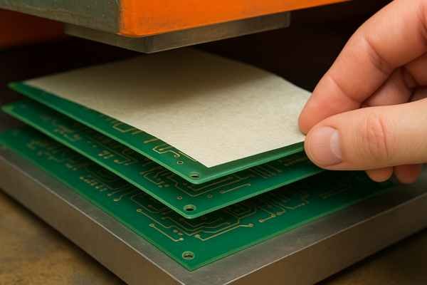
Without prepreg, creating robust, reliable multi-layer printed circuit boards as we know them would be impossible. I've relied on its properties in countless designs.
Prepreg Function and Characteristics
| Function | Description | Key Characteristic |
|---|---|---|
| Bonding Layers | Adheres copper foils to cores, or cores to other cores, during lamination. | B-stage resin liquefies, flows, and then cures under heat & pressure (e.g., 170-200 degrees C for FR-4). |
| Forming Dielectric Layers | The cured prepreg itself becomes an insulating layer between copper patterns. | Dielectric constant (Er) and thickness influence impedance and insulation. |
| Providing Insulation | Electrically isolates adjacent conductive layers and traces. | High dielectric strength. |
| Filling Gaps / Encapsulation | Resin flow fills voids in etched copper patterns, ensuring a solid, void-free structure. | Good flow properties are essential. |
| Achieving Target Thickness | Multiple plies of different prepreg styles (e.g., 106, 1080, 2116, 7628) are used to achieve desired thicknesses. | Each style has a nominal cured thickness (e.g., 1080 style approx. 0.06-0.075 mm / ply). |
The selection of prepreg types and the number of plies is a critical part of stackup design, especially when aiming for precise impedance control and overall board thickness.
What is FR-4 material?
You hear the term "FR-4" constantly when discussing PCBs. It's the bedrock of a vast majority of electronic products. But what exactly is this ubiquitous material?
FR-4 is a common NEMA (National Electrical Manufacturers Association) grade designation for glass-reinforced epoxy laminate sheets that are flame retardant (FR). It's the most widely used dielectric material for printed circuit boards due to its excellent balance of low cost, good mechanical strength, and adequate electrical insulating properties for many applications.
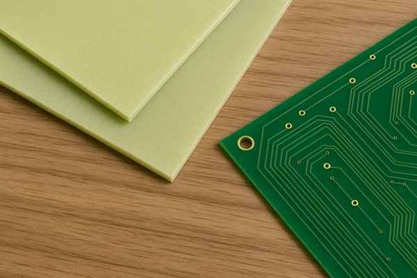
Throughout my career, FR-4 has been the default choice unless very specific high-frequency or thermal requirements dictated otherwise.
FR-4 Properties: Standard vs. High-Tg
| Property | Standard FR-4 | High-Tg FR-4 | Importance |
|---|---|---|---|
| Glass Transition Temp (Tg)6 | approx. 130 degrees C - 140 degrees C | approx. 170 degrees C - 180 degrees C (or higher) | Higher Tg means better thermal stability, especially for lead-free soldering. |
| Dielectric Constant (Er) | approx. 4.0 - 4.8 (at 1 GHz, varies) | Similar to standard FR-4, but check datasheet | Affects impedance and signal speed. (Source: IPC-4101E for general FR-4 types) |
| Loss Tangent (tan delta) | approx. 0.015 - 0.025 (at 1 GHz, varies) | Similar to standard FR-4, but check datasheet | Signal loss in dielectric. (Source: IPC-4101E) |
| Decomposition Temp (Td) | approx. 300 degrees C - 320 degrees C | greater than 340 degrees C (typically) | Temperature at which material chemically decomposes. |
| Primary Benefit | Lowest cost, widely available | Better performance in high-temp processes/apps | Cost vs. thermal performance trade-off. |
| Typical Use | General consumer & industrial electronics | Lead-free assembly, automotive, demanding env. | I often spec High-Tg FR-4 for reliability in harsher conditions. |
Always refer to the specific laminate manufacturer's datasheet (e.g., Isola, Panasonic, Shengyi) for precise values, as FR-4 properties can vary significantly between suppliers and product grades.
What are the 3 main types of core materials?
While FR-4 is the workhorse for many PCB applications, it's not the only option. Specialized applications often demand core materials with enhanced properties.
Beyond standard FR-4, three other main categories of core materials are: 1. High-frequency laminates (e.g., Rogers, Taconic) for RF/microwave needs, 2. Metal-core PCBs (MCPCBs) for superior thermal management, and 3. Flexible core materials (e.g., Polyimide) for dynamic or conformable circuits.
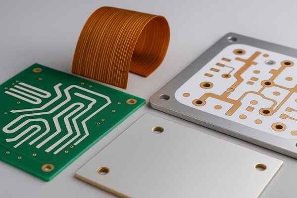
Choosing the right core material is fundamental. For a high-frequency Wi-Fi module redesign at Honeywell, specialized RF laminates were essential.
Comparison of Specialized Core Materials
| Core Material Type | Examples | Key Characteristics | Typical Applications |
|---|---|---|---|
| High-Frequency Laminates | Rogers RO4000 series (e.g., RO4350B), Taconic RF series, Arlon DiClad | Low dielectric loss (tan delta less than 0.005), stable Er over frequency (e.g., RO4350B Er = 3.48 +/-0.05). | RF/microwave circuits (antennas, PAs), high-speed digital (greater than 10 Gbps). |
| Metal-Core PCBs (MCPCBs) | Aluminum-backed, Copper-backed | Excellent heat dissipation (thermal conductivity 1-12 W/mK vs approx. 0.25 W/mK for FR-4). | LED lighting, power supplies, motor drives, automotive. |
| Flexible Core Materials | Polyimide (PI, e.g., Kapton), Polyester (PET) | Thin, bendable, durable for dynamic flexing (PI). PI Tg greater than 200 degrees C. Film thickness 12.5 um - 125 um. | Wearables, medical devices (infusion pumps), automotive, aerospace, mobile phones. |
Each of these materials addresses specific challenges that standard FR-4 cannot easily meet, whether it's maintaining signal integrity at gigahertz frequencies, managing high thermal loads, or allowing the circuit to bend and flex.
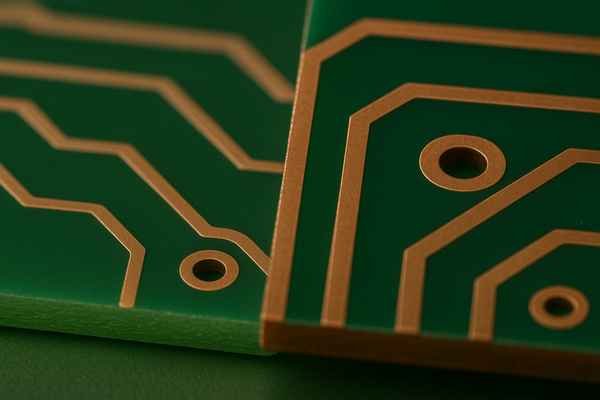
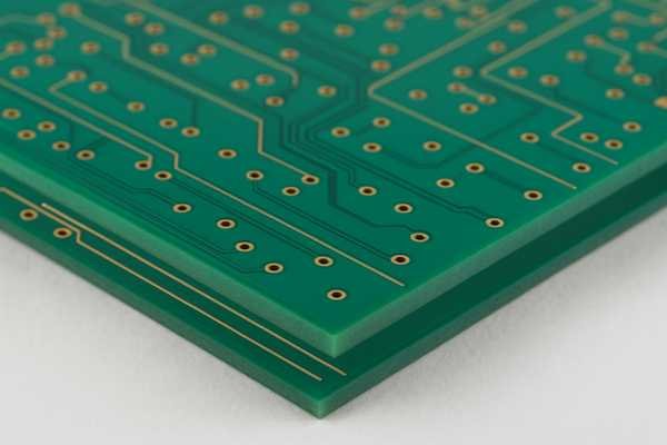
What is the difference between PCB stackup and buildup?
In the world of PCB design and manufacturing, "stackup" and "buildup" are related but distinct terms. Understanding the difference is especially important when dealing with modern, high-density designs.
"PCB stackup" refers to the general arrangement of copper and dielectric layers in any printed circuit board. "Buildup" or "sequential buildup (SBU)" specifically describes a manufacturing process used for High-Density Interconnect (HDI) PCBs, where layers with microvias are added sequentially.
While every PCB has a stackup, not every PCB is made using a buildup process. Buildup technology is a specialized subset of PCB manufacturing.
Stackup vs. Buildup Technology
| Feature | PCB Stackup (General) | Buildup Technology (HDI Specific) |
|---|---|---|
| Definition | The overall layer arrangement in any PCB. | A sequential manufacturing process for HDI PCBs, adding layers with microvias one by one (or in pairs). |
| Scope | Applies to all PCBs (2-layer to N-layer, rigid, flex). | Specific to HDI PCBs requiring high routing density. |
| Key Element | Order, thickness, and material of all layers. | Use of microvias7 (less than or equal to 150 um / 6 mils, often laser-drilled), sequential lamination. (Source: IPC-2226) |
| Manufacturing | Can be conventional lamination for non-HDI boards. | Involves multiple lamination cycles for buildup layers. |
| Example | A 6-layer board: SIG/GND/SIG/SIG/PWR/SIG is a stackup. | A 1+N+1 HDI structure (1 buildup layer on each side of an 'N' layer core). |
My work on the Honeywell Tuxedo Keypad platform leveraged HDI buildup techniques (like 1+N+1 or 2+N+2 structures) to accommodate fine-pitch BGAs and achieve the required component density in a sleek enclosure.
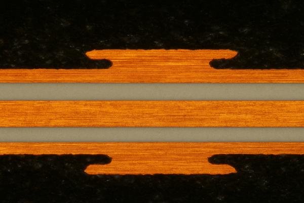
What is the difference between 1 oz and 2 oz copper PCB?
When specifying a PCB, you'll encounter terms like "1 oz copper" or "2 oz copper." This refers to the thickness of the copper foil used for the conductive layers, and it has significant implications.
The "oz" (ounce) in this context refers to the weight of copper spread over an area of one square foot. 1 oz copper has a nominal thickness of approximately 35 um (1.37 mils). 2 oz copper is twice as thick, roughly 70 um (2.74 mils), enabling it to carry more electrical current and dissipate more heat.
Choosing between 0.5 oz, 1 oz, 2 oz, or even heavier copper is a critical design decision I make based on current demands, thermal loads, and signal types.
Copper Weight Comparison
| Copper Weight | Approx. Thickness (um) | Approx. Thickness (mils) | Typical Applications | Relative Ampacity (Illustrative for same width) | Min. Trace/Space (Typical Guide) |
|---|---|---|---|---|---|
| 0.5 oz | approx. 17.5 um | approx. 0.69 mils | Internal signal layers, high-density routing | Base | 3/3 mils (0.075mm) |
| 1.0 oz | approx. 35 um | approx. 1.37 mils | General purpose internal/external layers, moderate power | approx. 1.4 - 1.6x of 0.5 oz | 4/4 mils (0.1mm) |
| 2.0 oz | approx. 70 um | approx. 2.74 mils | Power planes, high-current traces, thermal management | approx. 1.8 - 2x of 1.0 oz | 7/7 mils (0.175mm) |
| greater than or equal to 3.0 oz | greater than or equal to 105 um | greater than or equal to 4.11 mils | Very high power applications, bus bars, planar magnetics | Significantly Higher | greater than or equal to 10/10 mils (0.25mm) |
Note: Ampacity and Min. Trace/Space are general guidelines and can vary significantly based on PCB manufacturer capabilities, design specifics, and environmental conditions. Always consult IPC-2152 for ampacity calculations.
How do you choose PCB copper thickness?
Selecting the appropriate copper thickness for your PCB layers isn't arbitrary; it's a deliberate engineering decision that impacts performance, reliability, and cost.
Choose PCB copper thickness primarily based on the maximum current the traces need to carry (using IPC-2152 guidelines), the type of signals (thinner copper can be better for fine-pitch high-frequency signals), thermal dissipation requirements for power components, and manufacturing DFM (Design for Manufacturability) constraints, including cost and minimum feature sizes.
During my career, I've balanced these factors for diverse applications.
Factors for Selecting Copper Thickness
| Factor | Consideration | Typical Copper Choice | My Approach |
|---|---|---|---|
| Current Carrying Capacity | Max current per trace, acceptable temperature rise. (Governed by IPC-2152 standard). | 1 oz, 2 oz, or heavier. | Always use IPC-2152 for power traces; critical for motor drives in medical pumps. |
| Signal Type/Frequency | High-density routing, fine-pitch components, controlled impedance. Skin effect at very high frequencies. | 0.5 oz or 1 oz for signals. | Thinner copper for fine lines; surface roughness more critical than thickness for greater than 10-20GHz. (Source: Bogatin) |
| Thermal Management8 | Heat dissipation from power components. Larger copper areas and thicker copper spread heat better. | 2 oz or heavier for planes. | Used thicker copper for LED arrays and power stages to improve reliability. |
| Cost | Thicker copper increases material and processing costs. | Balance performance & cost. | Standard 1 oz is a good default if no special requirements. |
| Manufacturability (DFM)9 | Minimum trace/space achievable. Finer features with thinner copper. | Match to fab capability. | 0.5 oz for HDI; 2 oz might limit to 7/7 mil trace/space. Discuss with fabricator. |
| Layer Assignment | Outer layers might need more robust copper for pads/vias. Inner planes might carry significant current. | Varies per layer. | Outer: 1-2 oz. Inner Signal: 0.5-1 oz. Inner Plane: 1-2 oz. |
By carefully weighing these factors, I can engineer a PCB stackup with the right copper thicknesses to meet all performance, thermal, and cost objectives.
What is the best stack up for a 4-layer PCB?
A 4-layer PCB is a very common configuration, offering a significant step up in performance from 2-layer boards without the much higher cost of 6+ layer boards. But is there a single "best" stackup?
A widely recommended and often "best" 4-layer PCB stackup for good signal integrity and EMI control is: Signal (Top) / Ground Plane (GND) / Power Plane (PWR) / Signal (Bottom). This configuration provides excellent shielding and low-impedance return paths for signals.
I've used this classic 4-layer stackup in numerous projects because it provides a robust foundation. (Based on typical FR-4 Er approx. 4.2 for impedance estimates).
Recommended 4-Layer Stackup (SIG/GND/PWR/SIG)
| Layer | Name | Primary Function | Benefits |
|---|---|---|---|
| 1 | Signal (Top) | Component placement, routing critical/high-speed signals. | Signals reference Layer 2 (GND) for good integrity. |
| 2 | Ground (GND) | Solid ground plane. | Provides low-impedance return path for Layer 1, shields Layer 1 from Layer 3/4. |
| 3 | Power (PWR) | Solid power plane (or split planes). | Distributes power with low impedance, reference for Layer 4, shields Layer 4 from Layer 1/2. |
| 4 | Signal (Bottom) | Secondary components, routing less critical signals. | Signals reference Layer 3 (PWR) for good integrity. |
Dielectric Thickness Goals:
- L1-L2 (Signal to GND): Thin (e.g., 4-8 mils / 0.1-0.2 mm) for tight coupling.
- L2-L3 (GND to PWR): Thicker (core material, e.g., 30-50 mils / 0.76-1.27 mm for a 1.6mm board). Provides board capacitance.
- L3-L4 (PWR to Signal): Thin (e.g., 4-8 mils / 0.1-0.2 mm) for tight coupling.
This symmetrical arrangement offers the best balance of performance for most general-purpose and many high-speed digital designs on a 4-layer board.
What is the tolerance for PCB Stackup?
When I design a PCB stackup, I specify nominal thicknesses for each dielectric layer and the overall board. However, manufacturing processes inherently have variations. Understanding these tolerances is crucial.
Overall PCB thickness tolerance is typically +/-10% of the nominal thickness, as per IPC-A-600 Class 2 ("Acceptability of Printed Boards"). For individual dielectric layers, the tolerance of a manufactured core is tighter (e.g., +/-5% to +/-10%) than that of a pressed prepreg layer (which can be +/-10% to +/-20% or more, depending on thickness and complexity).
These tolerances directly impact the final characteristic impedance of traces.
Typical PCB Manufacturing Tolerances
| Parameter | IPC-A-600 Class 2 Tolerance (Typical) | Notes | Importance for Stackup |
|---|---|---|---|
| Overall Board Thickness | +/-10% of nominal | For 1.57mm (0.062") board: 1.413mm - 1.727mm. | Affects mechanical fit, overall stiffness. |
| Core Dielectric Thickness | +/-5% to +/-10% (from laminate mfr.) | E.g., Isola FR406: +/-0.018mm for 0.200mm core. (Source: Isola Datasheet) | More precise, good for predictable impedance if traces reference core copper. |
| Pressed Prepreg Thickness | +/-10% to +/-20% (or more for thin plies) | E.g., A single 1080 ply (nom. 2.5 mils) might vary +/-0.5 mil. (Source: Coombs & Holden) | Largest variable in dielectric thickness, critical for impedance control on outer layers. |
| Copper Foil Thickness | +/-5% to +/-10% (base foil) | For 1 oz (35um) copper: +/-1.75um to +/-3.5um. | Impacts final trace thickness, impedance, and current capacity. |
| Trace Width (Etched) | Varies with copper weight & fab | Typically +/-10% to +/-20% of nominal width. | Directly impacts impedance along with dielectric height. |
| Characteristic Impedance | Target +/-10% (common), +/-5-7% (tight) | Achieved by controlling H (dielectric height), W (trace width), Er (dielectric constant), and copper thickness. Requires careful design & fab control. | A 10% change in dielectric height (H) can shift Z0 (characteristic impedance) by approx. 5-6%. |
For any design requiring tight impedance control (e.g., 50 Ohms +/-5%), it's essential to communicate these needs clearly to your PCB fabricator and discuss their specific capabilities and material choices.
Conclusion
A meticulously planned PCB stackup isn't just a mechanical detail; it's fundamental to your circuit's electrical performance, EMI compliance, and overall reliability. Getting it right early saves headaches later.
-
Understanding Signal Integrity is crucial for high-speed designs, ensuring minimal crosstalk and stable performance. Explore more to enhance your PCB design skills. ↩
-
EMI/EMC Control is vital for compliance and performance. Discover how to effectively shield your designs from interference. ↩
-
Power Integrity ensures reliable performance in sensitive circuits. Learn more to optimize your designs for better power management. ↩
-
Understanding the Dielectric Constant is essential for optimizing signal integrity and impedance in PCB designs, especially for high-frequency applications. ↩
-
Exploring Loss Tangent helps in assessing signal loss, which is vital for ensuring reliable performance in high-speed electronic circuits. ↩
-
Understanding Tg is crucial for selecting materials that withstand high temperatures, especially in lead-free soldering applications. ↩
-
Learn about microvias, their manufacturing process, and their significance in high-density interconnect technology. ↩
-
Exploring thermal management strategies can help you design more reliable PCBs, especially for high-power applications. ↩
-
Learning about DFM can enhance your PCB designs, ensuring they are not only functional but also cost-effective and manufacturable. ↩


