 Skip to content
Facing RF signal problems? Unreliable performance and noise can derail your project. Strategic PCB design is your solution.
Key actions include meticulous impedance control, selecting low-loss materials, optimizing trace/via design, and ensuring robust grounding. Strategic via fencing and stitching, treated as critical components, are vital for superior electromagnetic isolation and signal integrity.
These fundamental steps are crucial. But to truly master RF PCB design, we need to explore specific challenges and their solutions in more detail. Let's dive deeper into common issues and how to address them effectively.
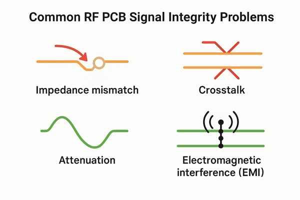
What are frequent signal integrity problems on RF PCBs?
RF circuits misbehaving? Unexpected noise or signal loss can be frustrating. Knowing common culprits is the first step to cleaner signals.
Frequent RF PCB signal integrity problems include impedance mismatches causing reflections, excessive signal loss (attenuation), crosstalk between traces, electromagnetic interference (EMI), and issues from non-ideal vias or ground planes.
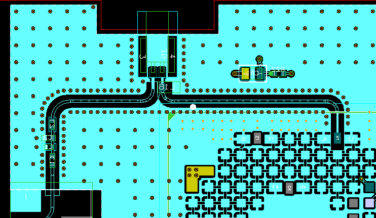
Identifying the Culprits: A Closer Look at Common RF Signal Integrity Problems
In my nearly 20 years as an embedded hardware engineer, I'veseen many RF projects struggle due to overlooked signal integrity issues. These problems aren't just academic; they have real-world consequences, delaying schedules and increasing costs.
Here's a breakdown of some frequent offenders:
| Problem Area | Typical Cause(s) | Key Impact on RF Performance |
|---|---|---|
| Impedance Mismatches1 | Incorrect trace geometry, poor connector launch, component pad variations | Signal reflections, reduced power transfer, VSWR issues, distortion |
| Signal Attenuation2 | High-loss dielectric material, excessive trace length, skin effect, copper roughness | Weak signals at receiver, reduced range, poor sensitivity |
| Crosstalk3 | Traces too close, poor grounding, long parallel runs | Unwanted signal coupling, noise, data errors, false triggering |
| EMI (Interference) | Inadequate shielding, ground loops, noisy components, poor layout | Radiated emissions (failing compliance), susceptibility to external noise |
| Non-Ideal Vias | Long stubs, insufficient ground return vias, high inductance/capacitance | Reflections, signal loss, impedance discontinuities |
| Ground Plane Issues | Discontinuities (slots/splits), insufficient stitching, high impedance | Unstable reference, ground bounce, increased noise, EMI radiation |
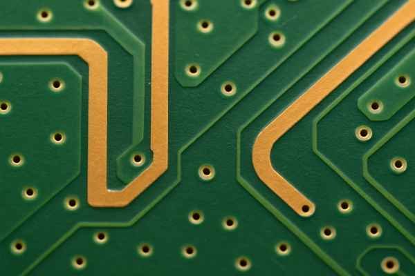
Understanding these common problems is the first step towards designing robust and reliable RF PCBs. As I'll discuss, thoughtful design of structures like via fences is paramount for mitigating many of these.
How does controlled impedance prevent RF signal degradation?
Signals weakening or reflecting unexpectedly? Uncontrolled impedance could be to blame. Consistent impedance is key for RF performance.
Controlled impedance ensures maximum power transfer and minimizes signal reflections by matching the trace's characteristic impedance to the source and load. This prevents signal degradation, distortion, and energy loss in RF circuits.
The Foundation of RF Clarity: How Controlled Impedance Works
Controlled impedance is fundamental in RF PCB design. Think of a signal traveling down a trace; it 'sees' an instantaneous impedance, known as the characteristic impedance (\(Z_{0}\)). If this \(Z_{0}\) changes abruptly, or if it doesn't match the impedance of the RF source or the load (like an antenna or an IC pin), a portion of the signal energy reflects. This is bad. Reflections cause signal distortion, reduce the power delivered, and can even damage sensitive components. For most RF applications, a target characteristic impedance of \(50 \Omega\) is a widely adopted standard, as documented in standards like IPC-2141A4, "Design Guide for High-Speed Controlled Impedance Circuit Boards."
The value of \(Z_{0}\) depends on the physical geometry of the trace and the properties of the PCB dielectric material. Here's how key parameters influence it for a typical microstrip trace:
| Parameter Change | Effect on Characteristic Impedance (\(Z_{0}\)) | Reason (Simplified) |
|---|---|---|
| Increase Trace Width (\(w\)) | Decreases \(Z_{0}\) | More area for fields, lower inductance, higher capacitance |
| Increase Dielectric Height (\(h\)) | Increases \(Z_{0}\) | Fields spread further, lower capacitance, higher inductance |
| Increase Dielectric Constant (\(D_{k}\)) | Decreases \(Z_{0}\) | Stronger field concentration, higher capacitance |
| Increase Copper Thickness (\(t\)) | Slightly Decreases \(Z_{0}\) | Minor effect, more pronounced for very thin dielectrics |
Precise calculation often involves formulas like Wheeler's or Wadell's, or more accurately, field solvers in EDA tools. By carefully controlling these parameters during PCB manufacturing, we ensure the trace maintains the desired \(Z_{0}\) (e.g., \(50 \Omega \pm 10\%\) or even tighter, like \(\pm 5\%\) for critical applications) along its entire length, preventing signal degradation.
Which PCB material electrical properties most affect RF signal loss?
RF signals dying out too quickly? Your PCB material might be absorbing energy. Choosing low-loss dielectrics is critical for RF.
The dissipation factor (\(\tan\delta\)) or loss tangent and the dielectric constant (\(D_{k}\)) of PCB materials most affect RF signal loss. Lower \(\tan\delta\) reduces dielectric losses, while stable \(D_{k}\) ensures consistent impedance.
Beyond FR-4: Choosing PCB Materials for Optimal RF Signal Transmission
When an RF signal travels through a PCB, some of its energy is lost in the dielectric material itself (dielectric loss) and some in the copper traces (conductor loss). Two key electrical properties of the PCB laminate dictate these losses:
-
Dissipation Factor5 (\(\tan\delta\)), also known as Loss Tangent: This is a measure of how much electromagnetic energy is absorbed by the dielectric material and converted into heat. A lower \(\tan\delta\) means less dielectric loss. For RF applications, especially at microwave frequencies (above \(1 \text{ GHz}\)), materials with a low \(\tan\delta\) are essential. Standard FR-4, a common PCB material, has a relatively high \(\tan\delta\), often around \(0.015 \text{ to } 0.025\) at \(1 \text{ GHz}\), making it unsuitable for many high-frequency RF applications. In contrast, specialized RF materials like Rogers RO4350B have a \(\tan\delta\) around \(0.0031 \text{ to } 0.0037\) at \(10 \text{ GHz}\) (per Rogers Corp. datasheets). This difference is huge for signal strength.
-
Dielectric Constant6 (\(D_{k}\) or \(\epsilon_{r}\)): This affects the impedance of traces and the propagation speed of signals. While not directly a loss factor, its stability over frequency and temperature is critical. Variations in \(D_{k}\) can cause impedance mismatches, leading to reflections and perceived loss. For RF, you want a \(D_{k}\) that's low and stable. For example, Rogers RO4350B has a design \(D_{k}\) of \(3.66\) at \(10 \text{ GHz}\), which is relatively stable. FR-4's \(D_{k}\) can vary significantly with frequency and manufacturing, typically ranging from \(4.0 \text{ to } 4.8\).
The following table gives a general idea for material selection:
| Material Type | Typical \(D_{k}\) (@\(10\text{GHz}\), process dep.) | Typical \(\tan\delta\) (@\(10\text{GHz}\), process dep.) | Suitability for RF |
|---|---|---|---|
| Standard FR-4 | \(\approx 4.0 - 4.7\) | \(\approx 0.015 - 0.020\) | Low frequency RF (\(<1 \text{ GHz}\)), cost-sensitive |
| Rogers RO4003C | \(3.38\) | \(0.0027\) | Excellent, up to millimeter-wave |
| Rogers RO4350B | \(3.48\) | \(0.0037\) | Very good, widely used for cellular, microwave |
| PTFE-based (e.g. Rogers RT/duroid 5880) | \(\approx 2.2\) | \(\approx 0.0009\) | Extremely low loss, high performance, expensive |
Choosing the right material based on its \(D_{k}\) and \(\tan\delta\) at your operating frequency is a foundational step in managing RF signal loss. Always consult specific manufacturer datasheets for precise values.
How can RF trace width and spacing be set for optimal signals?
Traces too close or wrong width? This can lead to impedance issues and crosstalk. Proper dimensions are vital for RF signals.
RF trace width is set to achieve the target characteristic impedance (e.g., \(50 \Omega\)) based on PCB material and stack-up. Spacing is determined by crosstalk limits, often using the "\(3W\) rule" (edge-to-edge spacing \(\geq 3 \times\) trace width) as a starting point, but requiring more for RF.
Width and Gaps: Setting Trace Dimensions for Impedance and Crosstalk Control
Setting the correct trace width and spacing is critical for maintaining signal integrity in RF PCBs. These dimensions directly influence impedance and crosstalk.
Trace Width for Impedance Control:
As I discussed earlier, trace width (\(W\)) is a primary factor in determining characteristic impedance (\(Z_{0}\)). For a given PCB material (with known \(D_{k}\) and height \(h\) to the reference plane), and a target \(Z_{0}\) (usually \(50 \Omega\)), the trace width \(W\) can be calculated using formulas or, more accurately, with EDA tools that include field solvers. For example, on a standard \(1.6\text{mm}\) FR-4 board with a \(D_{k}\) of \(4.5\) and a \(0.2\text{mm}\) dielectric thickness to the ground plane, a \(50 \Omega\) microstrip trace might be around \(0.35\text{mm to }0.4\text{mm}\) wide. For lower \(D_{k}\) RF materials, the trace width for \(50 \Omega\) will generally be wider for the same dielectric thickness. It's crucial to get this right to avoid reflections.
Trace Spacing for Crosstalk Reduction:
Crosstalk occurs when electromagnetic fields from one trace (the aggressor) couple onto an adjacent trace (the victim). To minimize this, we need adequate spacing.
| Spacing Guideline/Strategy | Typical Target Isolation | Notes |
|---|---|---|
| \(3W\) Rule (Digital) | \(\approx -25\text{dB to } -40\text{dB}\) | Edge-to-edge spacing \(\geq 3W\). Often insufficient for sensitive RF. |
| \(5W\) Rule or \(3H\) Rule (RF) | \(\approx -40\text{dB to } -60\text{dB}\) | Spacing \(\geq 5W\), or \(\geq 3H\) (where \(H\) is dielectric height). Better for RF. |
| Guard Traces | Can improve by \(10\text{dB}-20\text{dB+}\) | Grounded trace between signals, needs frequent via stitching to ground. |
| Via Fences | Can improve by \(20\text{dB+}\) | Rows of ground vias alongside traces/blocks. Very effective for RF isolation. |
For RF signals, especially at higher frequencies or with very sensitive lines, the \(3W\) rule is often insufficient. I've found that a \(5W\) rule or even greater spacing (e.g., spacing equal to 3 to 5 times the height \(H\) of the trace above the ground plane) might be necessary. The goal is to keep aggressor-victim coupling below an acceptable threshold, typically \(-30\text{dB to } -60\text{dB}\) or better for many RF applications. Simulation is often the best way to verify spacing for critical RF lines.
What is a key best practice for RF via design?
Vias causing signal reflections or losses? Poor via design can cripple RF performance. Optimizing vias is essential for high frequencies.
A key best practice for RF via design is to minimize their inductive and capacitive parasitics. This involves using multiple ground return vias close to the signal via and keeping via stubs short.
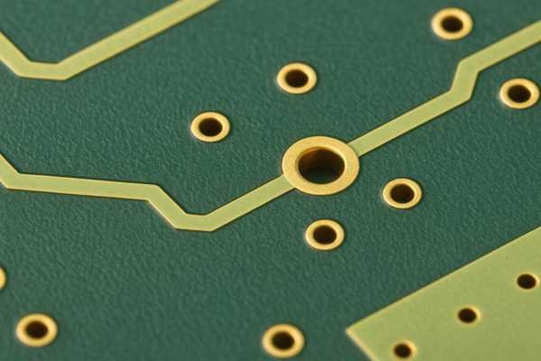
Vias: Not Just Holes, But Key RF Pathway Elements
Vias are necessary for routing signals between different PCB layers, but they are also discontinuities that can wreak havoc on RF signals if not designed properly. At high frequencies, a via doesn't act like a simple short circuit. It introduces parasitic inductance and capacitance7, which can cause impedance mismatches, reflections, and signal loss. My experience has taught me that treating vias with as much care as traces is vital.
| Via Design Parameter | RF Impact | Best Practice Guideline |
|---|---|---|
| Ground Return Vias | Inadequate return path increases inductance, EMI | Place 2-4 ground vias symmetrically around signal via, spacing \(<1\text{mm}\) if possible |
| Via Stub Length | Resonances, reflections at high frequencies | Minimize stub length; use back-drilling for critical signals (frequencies greater than a few \(\text{GHz}\)) |
| Via Diameter/Pad Size | Affects parasitic capacitance and inductance | Use smallest feasible size; balance with manufacturing & current needs |
| Anti-pad Diameter | Affects via impedance | Optimize for target impedance (e.g., \(50 \Omega\)) through the via structure |
| Number of Vias (parallel) | Reduces inductance for power/ground | Use multiple vias for low-inductance connections to planes |
A key best practice is to ensure a continuous and low-inductance return path for the RF current. When a signal via transitions layers, its return current in the ground plane also needs to transition. This is achieved by placing ground stitching vias very close to the signal via. Typically, I aim for 2 to 4 ground vias surrounding the signal via. The distance between the signal via and these ground vias should be minimized, often as close as manufacturing rules allow, perhaps \(0.5\text{mm to }1.0\text{mm}\) center-to-center.
Another critical aspect is minimizing via stub length8. For critical RF signals, especially above a few \(\text{GHz}\), back-drilling is often used. As part of my core insight, treating these via structures, especially in via fences, as full-fledged RF components requiring co-simulation is key for predictable high-frequency performance.
How are RF signal reflections due to impedance mismatch reduced?
Signals bouncing back and causing chaos? Impedance mismatches are common culprits. Matching is key to taming reflections.
RF signal reflections are reduced by ensuring a consistent characteristic impedance (typically \(50 \Omega\)) along the entire signal path, from source, through traces and connectors, to the load. Matching networks can also be used.
Stopping Signal Bounce-Back: Strategies for Reducing RF Reflections
Signal reflections are a major source of problems in RF circuits. They occur whenever a signal encounters a change in impedance. The measure of this reflection is often given by S-parameters9, specifically \(S_{11}\) (return loss). An \(S_{11}\) of \(0 \text{ dB}\) means all power is reflected, while a value like \(-20 \text{ dB}\) (1% power reflected) is good, and \(-25 \text{ dB to } -30 \text{ dB}\) is often targeted for high-performance systems.
| Mismatch Cause | Mitigation Technique | Key Consideration |
|---|---|---|
| Incorrect Trace Impedance | Precise trace width/spacing, controlled dielectric | Use field solvers, verify with PCB manufacturer |
| Poor Connector Launch | Manufacturer recommended footprint, impedance modeling | Smooth transition from PCB trace to connector pin |
| Component Pad Discontinuities | Optimized pad shapes, ground cutouts under pads | Reduce excess capacitance or inductance at component mount |
| Via Transitions | Optimized via design, ground return vias | Maintain impedance through the via structure |
| Source/Load Impedance Differs from System | Impedance matching network (\(L-C\), stubs) | Design for target frequency band, minimize network loss |
The primary way to reduce reflections is to maintain a constant characteristic impedance (usually \(50 \Omega\)) throughout the signal path. This includes PCB traces, connectors, component pads, and layer transitions via vias.
If impedance mismatches are unavoidable (e.g., an antenna has an impedance of \(75 \Omega\) while the system is \(50 \Omega\)), then impedance matching network10s are used. These are typically small circuits made of inductors (\(L\)) and capacitors (\(C\)) placed close to the mismatch point. These networks transform the mismatched impedance to the desired system impedance over a specific frequency band, often designed using tools like Smith Charts or RF simulation software, as detailed in texts like Pozar's "Microwave Engineering."
What PCB layout technique best reduces RF crosstalk?
Signals jumping between traces? Crosstalk degrades RF performance and can cause failures. Strategic layout is your best defense.
The best PCB layout technique to reduce RF crosstalk involves maximizing space between parallel traces, using ground planes effectively, and employing shielding techniques like guard traces or, critically, well-designed via fences.
Keeping Signals Clean: Advanced Techniques for RF Crosstalk Reduction
Crosstalk, the unwanted coupling of signals between adjacent traces, is a persistent challenge in RF PCB layout. My primary strategy involves a combination of spacing and shielding.
| Crosstalk Shielding Method | Relative Effectiveness | Typical Implementation Complexity | Key Consideration |
|---|---|---|---|
| Increased Spacing (e.g., \(>5W\) or \(>3H\)) | Moderate to High | Low | Space permitting; fundamental first step |
| Orthogonal Routing | Moderate | Low to Moderate | For adjacent signal layers; reduces broadside coupling |
| Guard Traces | Moderate to High | Moderate | Grounded trace between signals; needs good stitching |
| Via Fences11/Walls | High to Very High | Moderate to High | Rows of ground vias; excellent for isolation |
| Stripline Configuration | High | Moderate | Signal trace embedded between two ground planes |
1. Maximize Spacing: The further apart traces are, the weaker the coupling. For RF, I typically aim for \(5W\) or even more (spacing \(\geq 5W\)), or spacing of at least 3 to 5 times the height \(H\) of the trace above its reference ground plane.
2. Effective Use of Ground Planes: A solid ground plane contains fields.
3. Guard Traces: A grounded trace run between signal traces, well-stitched to ground, can intercept coupling fields.
4. Via Fences (Stitching Vias): This is where my insight about treating via structures as critical components truly shines. For isolating RF traces or entire sections, via fences are extremely effective. A row of ground-stitching vias (spacing \(\frac{\lambda}{20}\text{ to }\frac{\lambda}{10}\) of the highest frequency, where \(\lambda\) is the wavelength) alongside a trace or around an RF block creates a "Faraday cage" effect. I insist on co-simulating via fence designs with the signal paths they protect, as their specific geometry (via diameter, spacing, depth, return path continuity) is critical for optimal performance, especially at higher frequencies (e.g., at \(10 \text{ GHz}\) in FR4, \(\lambda \approx 14\text{mm}\), so via spacing might be \(0.7\text{mm to }1.4\text{mm}\)) or in dense layouts. Generic rules of thumb are often not enough.
How is RF differential pair skew minimized in PCB layout?
Differential signals arriving out of sync? Skew can distort your high-speed RF data. Precise length matching is crucial.
RF differential pair skew is minimized by ensuring the electrical lengths of the two traces (\(P\) and \(N\)) are as identical as possible. This involves meticulous length matching in the layout, including compensating for bends and asymmetries.

In Perfect Step: Ensuring RF Differential Pair Integrity through Skew Minimization
Differential signaling offers excellent noise rejection, but its benefits rely on the two signals (\(P\) and \(N\)) being perfectly complementary and arriving simultaneously. Skew12 is the timing difference between them. Excessive skew degrades performance.
Key techniques for minimizing skew include:
- Identical Routing: Route \(P\) and \(N\) traces parallel and close, maintaining consistent differential impedance (e.g., \(100 \Omega\) or \(90 \Omega\)).
- Symmetrical Bends: Use symmetrical bend patterns.
- Length Compensation (Serpentine Traces): Add small "trombone" sections to the shorter trace. Design these carefully to avoid impedance issues; serpentine legs should be spaced \(>3W-5W\) apart (where \(W\) is trace width).
- Symmetrical Vias: Use vias symmetrically on both lines if needed.
The maximum allowable skew is critical and frequency-dependent.
| Data Rate / Approx. Nyquist Freq. | Bit Period | Typical Max Allowable Skew (Physical Length on FR4-like material, \(\approx 160\text{ ps/inch}\)) |
|---|---|---|
| \(1 \text{ Gbps / } 500 \text{ MHz}\) | \(1000 \text{ ps}\) | \(< 50 \text{ ps (\approx 7-8 mm or \approx 300 mils)}\) |
| \(5 \text{ Gbps / } 2.5 \text{ GHz}\) | \(200 \text{ ps}\) | \(< 10 \text{ ps (\approx 1.5 mm or \approx 60 mils)}\) |
| \(10 \text{ Gbps / } 5 \text{ GHz}\) | \(100 \text{ ps}\) | \(< 5 \text{ ps (\approx 0.75 mm or \approx 30 mils)}\) |
| \(25 \text{ Gbps / } 12.5 \text{ GHz}\) | \(40 \text{ ps}\) | \(< 1-2 \text{ ps (\approx 0.15-0.3 mm or \approx 6-12 mils)}\) |
For multi-gigabit signals, allowable skew can be just a few picoseconds. For instance, a \(10 \text{ Gbps}\) signal (\(100 \text{ ps}\) bit period) might tolerate only \(5 \text{ ps}\) of skew, translating to a physical length difference of about \(0.75 \text{ mm (30 mils)}\) on typical FR-4. Some high-speed interfaces demand skew matching down to \(1-2 \text{ mils (25-50 } \mu\text{m)}\). Always consult component datasheets for specific skew budget requirements.
Why is a continuous ground plane vital for RF signal quality?
RF signals acting erratically? A fragmented ground could be the invisible culprit. A solid ground is foundational for RF stability.
A continuous ground plane is vital for RF signal quality because it provides a stable, low-impedance return path for signals, minimizes ground loops, improves shielding, and helps maintain consistent characteristic impedance.
The Bedrock of RF Performance: Why a Continuous Ground Plane is Non-Negotiable
In my experience, a robust and continuous ground plane is one of the most critical aspects of successful RF PCB design.
| Ground Plane Issue | Consequence | Best Practice Remedy |
|---|---|---|
| Slots/Splits Under High-Speed Traces | Increased return path inductance, reflections, EMI radiation, crosstalk | Keep ground planes solid under critical traces; bridge splits carefully |
| Insufficient Ground Vias/Stitching | Poor inter-plane ground connection, ground bounce, reduced shielding | Use ample ground stitching vias, especially at edges & between blocks |
| High Impedance Ground Path | Noise coupling, unstable voltage reference | Maximize copper area for ground, use multiple layers if possible |
| Ground Loops13 | Unpredictable currents, noise pickup | Ensure a single, low-impedance common ground reference point/plane |
Here’s why it's so important:
- Low-Impedance Return Path: At RF, current returns via the path of least inductance, ideally directly under the signal trace on a solid ground plane. Disruptions force detours, increasing loop area, inductance, and causing reflections and EMI.
- Minimizing Ground Loops: Provides a common, low-impedance reference.
- Shielding: Acts as a shield, reducing EMI susceptibility and radiation.
- Consistent Impedance: Characteristic impedance calculations assume a solid reference plane.
- Reference for Via Stitching: Effective via stitching needs solid ground planes. Via stitching across the board, with spacing around \(\frac{\lambda}{10}\text{ to }\frac{\lambda}{20}\) of the highest frequency of interest (where \(\lambda\) is wavelength), ties ground planes tightly, ensuring a consistent low-impedance ground and improving isolation.
Avoid routing signals on ground planes. If splits are unavoidable (e.g., AGND/DGND), manage trace crossings carefully (e.g., capacitor bridge).
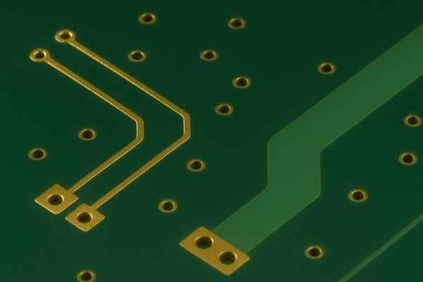
How do sharp trace bends impact high-frequency RF signals?
Using sharp 90-degree corners in RF traces? These can act like tiny mirrors, reflecting signals. Smooth bends are better for RF.
Sharp trace bends (e.g., 90-degree angles) in high-frequency RF signals can cause impedance discontinuities, leading to signal reflections and increased radiation. Smoother, chamfered, or rounded bends are preferred.
When an RF signal encounters a sharp bend, it's like hitting an impedance speed bump.
| Bend Type | Typical Impedance Discontinuity14 | Reflection Level (\(S_{11}\)) | Radiation Potential | Recommendation for RF (\(>1 \text{ GHz}\)) |
|---|---|---|---|---|
| Sharp 90-degree | Significant | High | Moderate to High | Avoid |
| Dual 45-degree (Chamfered) | Moderate | Low to Moderate | Low to Moderate | Acceptable, better than sharp |
| Curved (Radius \(R \geq 3W\)) | Minimal | Very Low | Low | Preferred / Ideal |
| Curved (Radius \(R \geq 5W\)) | Very Minimal | Negligible | Very Low | Best |
(Where \(W\) is trace width)
Effects of sharp bends:
- Signal Reflections15: The impedance discontinuity causes reflections (\(S_{11}\)).
- Increased Radiation: Sharp bends can act as small antennas, causing EMI.
- Local Impedance Changes: Sharp outer corners reduce effective width (increasing inductance), while inner corners increase local capacitance.
To mitigate these:
- Curved Bends: Ideal. Use a bend radius (\(R\)) at least three times the trace width (\(W\)) (so \(R \geq 3W\)). Larger (\(R \geq 5W\)) is even better.
- Chamfered Bends (45-Degree Bends): Two 45-degree bends are much better than one sharp 90-degree bend. A miter cutting the corner (diagonal \(\approx 1.5W\text{ to }3W\)) helps.
At \(\text{GHz}\) frequencies, these small discontinuities add up. I always advocate for smooth, sweeping bends for critical RF paths.
How does copper surface roughness affect RF signal loss?
Losing more signal than expected at high frequencies? The microscopic texture of your copper might be the issue. Smooth copper helps RF.
Copper surface roughness increases RF signal loss, especially at high frequencies, due to the skin effect. Rougher surfaces create longer current paths and increase conductor losses.
Surface Matters: How Copper Roughness Impacts High-Frequency RF Losses
At high frequencies, the skin effect16 forces RF currents to flow near the conductor's surface. Skin depth (\(\delta\)) decreases with frequency (e.g., for copper, \(\delta \approx 0.66 \mu\text{m at } 10 \text{ GHz}\) and \(\delta \approx 0.21 \mu\text{m at } 100 \text{ GHz}\)). If copper surface roughness17 (\(R_{z}\), average peak-to-valley) is comparable to or larger than \(\delta\), the current path along the "hills and valleys" is longer, increasing resistive losses.
| Copper Foil Type | Typical \(R_{z}\) (Peak-to-Valley Roughness) | Relative Conductor Loss at High Frequencies (\(>5-10 \text{ GHz}\)) | Typical Use Case |
|---|---|---|---|
| Standard Profile (STD) | \(5-10 \mu\text{m}\) (or more) | Highest | General purpose, lower frequency applications |
| Low Profile (LP) | \(\approx 3-5 \mu\text{m}\) | Moderate | Improved performance for some \(\text{GHz}\) applications |
| Very Low Profile (VLP) | \(\approx 1.5-3 \mu\text{m}\) | Low | Good for many high-speed digital and RF (\(10-40 \text{ GHz}\)) |
| Ultra-Low Profile (ULP) / Hyper Very Low Profile (HVLP) | \(< 1.5 \mu\text{m}\) | Lowest | Critical high-frequency, mmWave applications |
The increased loss can be modeled (e.g., Hammerstad and Jensen, Morgan models). At \(28 \text{ GHz}\), smoother copper might reduce conductor loss by \(10\%-30\%\) or more compared to standard rough copper. Specifying low-profile (LP, VLP, ULP) copper is a common requirement for designs operating well into the \(\text{GHz}\) range to manage these losses. Always check with your PCB fabricator about available copper foil types.
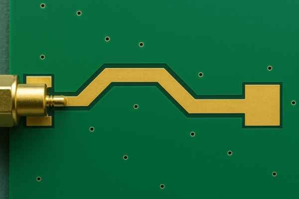
How can RF connector choice impact signal integrity?
RF signals degrading at the board edge? Your connector could be the bottleneck. Choosing the right RF connector is crucial.
RF connector choice impacts signal integrity through its impedance match (typically \(50 \Omega\)), frequency range, insertion loss, and return loss. A poorly chosen or improperly mounted connector can introduce significant mismatches and losses.
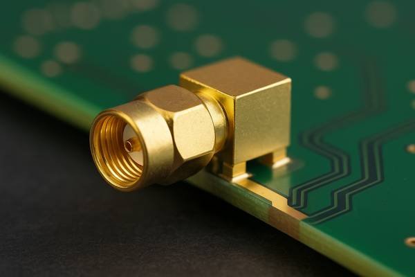
The Gateway: Selecting and Implementing RF Connectors for Optimal Signal Transfer
RF connectors are critical for signal integrity at the board interface.
| Connector Type | Typical Max Frequency | Common Impedance | Mating Style | Typical Application |
|---|---|---|---|---|
| U.FL / MHF | \(\approx 6 \text{ GHz}\) (series dep.) | \(50 \Omega\) | Snap-on | Internal, space-constrained |
| SMA | \(\approx 18 \text{ GHz}\) (std) | \(50 \Omega\) | Screw-on | General RF, test & measurement |
| SMB | \(\approx 4 \text{ GHz}\) | \(50 \Omega\) | Snap-on | Board-to-board, internal |
| SMP | \(\approx 20-40 \text{ GHz}\) | \(50 \Omega\) | Push/Snap-on | High-density, board-to-board |
| 2.92mm (K) | \(\approx 40 \text{ GHz}\) | \(50 \Omega\) | Screw-on | Precision, mmWave |
| 2.4mm | \(\approx 50 \text{ GHz}\) | \(50 \Omega\) | Screw-on | Precision, mmWave |
| 1.85mm (V) | \(\approx 67 \text{ GHz}\) | \(50 \Omega\) | Screw-on | Precision, mmWave |
Key factors:
- Impedance Match: Must be \(50 \Omega\) for most RF systems.
- Frequency Range: Use within specified limits.
- Insertion Loss (\(IL\)) & Return Loss (\(RL\))18: Aim for low \(IL\) (e.g., \(< 0.1 \text{ dB to } 0.3 \text{ dB}\)) and high \(RL\) (e.g., \(> 15 \text{ dB or } 20 \text{ dB}\)). Check datasheets (Molex, TE, Amphenol, Rosenberger).
- Launch Design: The PCB footprint must ensure a smooth \(50 \Omega\) transition. Manufacturers provide recommended footprints. A poor launch (e.g., improper trace width, missing ground cutouts under signal pin for some connector types) can severely degrade connector performance.
Skimping on connector quality or launch design is a false economy.
What basic RF component placement rule improves signal paths?
RF circuits struggling with noise or instability? Component placement might be disorganized. Strategic placement creates clean signal paths.
A basic RF component placement rule is to keep signal paths as short and direct as possible. Place critical RF components first, then group related analog and digital sections separately to minimize interference.
Location, Location, Location: Fundamental RF Component Placement Strategies
Component placement is crucial for RF PCB layout success.
| Placement Principle | Rationale | Impact if Ignored |
|---|---|---|
| Short & Direct RF Paths | Minimize loss, inductance, capacitance, delay, noise pickup | Increased attenuation, parasitics, potential instability |
| Prioritize Critical Paths | Ensure best performance for key signals (e.g., LNA input) | Degraded sensitivity, higher noise figure |
| Follow Signal Flow | Logical layout, minimizes crossovers, simplifies routing | Complex routing, longer traces, increased coupling |
| Group Related Circuitry | Keep functional blocks tight (e.g., matching nets at antenna) | Stray parasitics, compromised block performance |
| Isolate Noisy & Sensitive Sections | Prevent digital noise in RF, PA noise in LNA, etc. | Interference, desensitization, spurious signals |
| Short Paths to Ground | Minimize inductance for bypass caps, component grounding | Poor bypassing effectiveness, ground bounce |
My approach:
- Identify critical RF paths and place these components first for shortest connections.
- Arrange components logically, following signal flow.
- Group functional blocks (LNA, filters, PA) tightly.
- Isolate sections: High-power from low-power, digital from analog RF. Consider shielding cans for very sensitive areas.
- Ensure direct, low-inductance grounding for bypass capacitors and component ground pads, often using multiple vias straight to the ground plane.
Careful placement prevents many signal integrity headaches.
Conclusion
Solving RF PCB signal integrity means mastering impedance, materials, and layout. Crucially, optimizing via fences and stitching as critical components ensures robust electromagnetic isolation and superior signal performance.
-
Understanding impedance mismatches is crucial for optimizing RF performance and avoiding costly design errors. ↩
-
Exploring signal attenuation helps in designing better RF systems, ensuring stronger signals and improved range. ↩
-
Learning about crosstalk can help engineers implement effective strategies to reduce noise and improve data integrity. ↩
-
IPC-2141A provides essential guidelines for high-speed controlled impedance circuit boards, vital for any RF designer. ↩
-
Understanding the Dissipation Factor is crucial for selecting PCB materials that minimize energy loss in RF applications, ensuring better signal integrity. ↩
-
Exploring the role of Dielectric Constant helps in choosing materials that maintain signal quality and reduce reflections in RF circuits. ↩
-
Learning about parasitic effects can improve your PCB layout, leading to better performance and reliability. ↩
-
Exploring the impact of via stub length can help you optimize your designs for high-frequency applications. ↩
-
Understanding S-parameters is crucial for analyzing and improving RF circuit performance. Explore this link for in-depth insights. ↩
-
Impedance matching networks are vital for optimizing signal integrity. Discover their design and application in RF systems. ↩
-
Learning about via fences can help you implement advanced isolation techniques, crucial for high-frequency applications in RF designs. ↩
-
Understanding skew is crucial for optimizing differential signaling performance. Explore this link to learn more about its impact and management. ↩
-
Exploring ground loops will help you grasp their impact on RF performance and how to mitigate issues effectively. ↩
-
Understanding impedance discontinuity is crucial for optimizing RF signal integrity and minimizing reflections. ↩
-
Exploring the impact of signal reflections can help you design better RF circuits and improve performance. ↩
-
Understanding the skin effect is crucial for optimizing RF designs and minimizing losses in high-frequency applications. ↩
-
Exploring this topic can provide insights into material selection for better RF performance in high-frequency circuits. ↩
-
Understanding IL and RL is crucial for optimizing RF performance. Explore this link for expert insights and techniques. ↩


