 Skip to content
Are you designing a PCB for mass production and worried about testing? The wrong test point strategy can lead to costly fixture redesigns, production delays, and unreliable products, causing major headaches down the line.
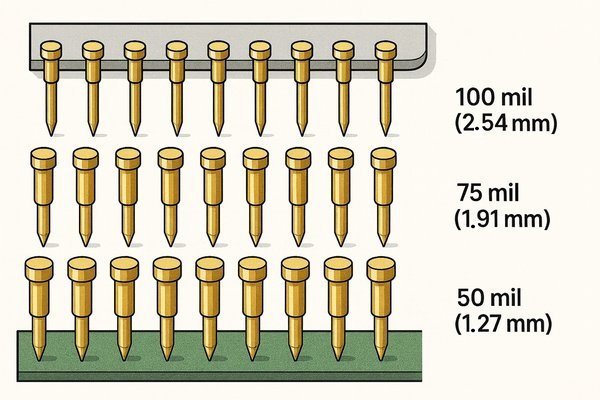
The most common standard pitch for bed-of-nails test fixtures is 100 mil (0.100 inches or 2.54 mm). While finer pitches like 75 mil (1.91 mm) and 50 mil (1.27 mm) are available for denser boards, they significantly increase the cost and complexity of the fixture and may reduce long-term reliability.
As a hardware engineer with nearly two decades of experience, I've seen how overlooking Design for Test (DFT) can derail a project. Proper planning for in-circuit testing (ICT) is not an afterthought; it's a critical step that ensures a smooth transition from prototype to mass production. Let's break down what you need to know to get it right.
What is a Bed-of-Nails Test Fixture?
Struggling to understand how you'll verify thousands of connections on your assembled boards quickly? Without an efficient method, you risk shipping defective products, leading to expensive recalls and a damaged reputation.
A bed-of-nails test fixture is a custom-built apparatus that uses an array of spring-loaded pins, known as "pogo pins," to make simultaneous electrical contact with numerous test points on a printed circuit board assembly (PCBA). This allows for rapid, automated in-circuit testing (ICT).
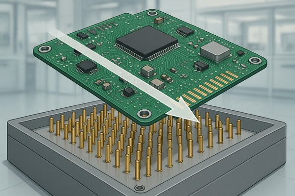
Think of it as a custom connector perfectly tailored to your board. The Device Under Test (DUT) is placed on the fixture, and an actuation mechanism pushes it down, ensuring every designated pogo pin connects securely with its corresponding test point on the PCB. Once connected, an automated tester can quickly check for a wide range of manufacturing defects.
Core Fixture Mechanics: Actuation and Alignment
A fixture isn't just a plate of pins. It's a precise mechanical system.
- Actuation: The force required to compress hundreds or thousands of pogo pins is significant. This is typically achieved in one of two ways: a vacuum fixture, which sucks the PCB down onto the pins, or a mechanical fixture (press-down), which uses levers or pneumatic presses. Vacuum fixtures are common but require a good seal around the board's edge.
- Alignment: Precision is ensured by tooling pins in the fixture that mate with tooling holes on the PCB. This guarantees the board is positioned with an accuracy often better than ±0.002 inches (0.05 mm).
What Defects Can ICT Find?
An ICT system is incredibly effective at finding the most common flaws that occur during PCB assembly. In addition to checking passive components, it can verify the placement and connection of integrated circuits by checking for shorts and opens on their pins and ensuring they are receiving power correctly. While it doesn't perform a full functional validation of the chip, it confirms the manufacturing process was sound.
| Defect Type | Description | Common Example |
|---|---|---|
| Shorts | An unintended electrical connection between two or more nets. | A solder bridge between two adjacent pins on an IC. |
| Opens | A break in a connection that should be continuous. | A component lead that did not properly solder to its pad (a "tombstone" resistor). |
| Component Value | A passive component (resistor, capacitor, inductor) is incorrect. | A 1kΩ resistor was placed where a 10kΩ resistor should be. |
| Missing Component | A component was not placed on the board by the pick-and-place machine. | An empty set of pads where a decoupling capacitor should be. |
| Reversed Component | A polarized component is installed backward. | A diode or electrolytic capacitor is oriented incorrectly. |
Choosing the Right Pogo Pin Head Style
Not all pogo pins are the same. The "head" or tip style is chosen based on what it will be contacting to ensure the most reliable electrical connection.
| Head Style | Best Use Case | Rationale |
|---|---|---|
| Serrated (Crown) | Standard test pads, vias | The sharp points cut through flux residue and oxides for a reliable connection. |
| Spear (Pointed) | Through-hole leads, small pads | Good for precise targeting but can be aggressive and leave a mark. |
| Flat Head | Connector pins, clean flat pads | Distributes pressure evenly to avoid damaging delicate surfaces. |
| Cupped | Round component leads/pins | Self-centers on the lead to ensure a secure connection. |
What are the Design Guidelines for Creating Test Points on a PCB?
Unsure how to properly design test points on your PCB? Poorly designed test points can be inaccessible or unreliable, making your board untestable, forcing a costly redesign, and delaying your entire production schedule.
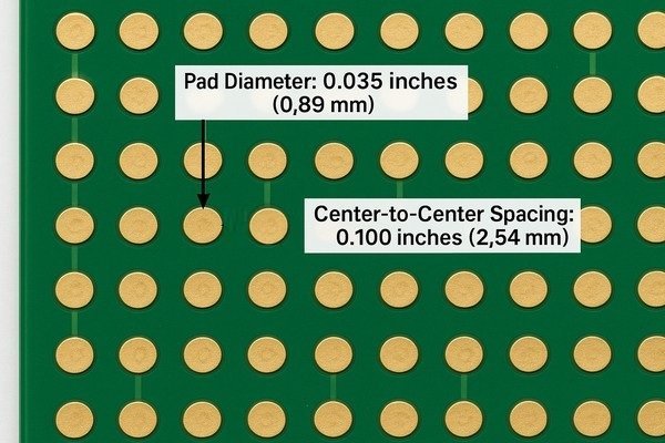
Effective test point design involves creating accessible, sufficiently large, and well-spaced pads. A general rule is to make test pads at least 0.035 inches (0.89 mm) in diameter and maintain a minimum center-to-center spacing of 0.100 inches (2.54 mm) to ensure reliable contact with standard test probes.
Integrating testability from the start is far more efficient than trying to add it later. Here are the key guidelines I follow, aligned with industry best practices like those found in the IPC standards.
Key Design for Test (DFT) Rules
| Guideline | Recommendation | Rationale |
|---|---|---|
| Test Point Size | Minimum 0.035" (0.89mm), ideally 0.040" (1.02mm) diameter. | Provides a large enough target for the pogo pin, accommodating for manufacturing tolerances in both the PCB and the fixture. |
| Test Point Spacing | Minimum 0.050" (1.27mm), ideally >0.100" (2.54mm) center-to-center. | Prevents shorting between adjacent probes and allows for the use of more robust, less expensive standard probes. |
| Shape | Square pads are preferred over round pads. | A square pad offers about 27% more surface area than a round pad of the same width, increasing the chances of a solid connection. |
| Location | Place all test points on one side of the PCB (typically the bottom). | This simplifies the test fixture design, making it significantly cheaper and faster to build. Dual-sided fixtures are complex and expensive. |
The Critical Deliverable: The Test Point Report
In addition to your Gerbers and BOM, you must provide a Test Point Report to your fixture house. This is a simple text file, often called a centroid file or XY file, that lists the exact coordinates of every test point. Each line should contain the Net Name, X-coordinate, Y-coordinate, and board side. This file is what the fixture designers use to program their high-precision drills to create the probe plate. An inaccurate report will lead to a completely non-functional fixture.
What is the Recommended Size and Shape for a Test Pad?
Choosing the wrong test pad size or shape seems like a minor detail, but it's not. If pads are too small, test probes will miss their mark, leading to false failures. This wastes valuable time on the production line as operators re-test and debug perfectly good boards.
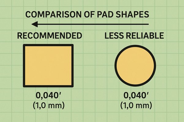
The recommended size for a reliable test pad is a diameter of 0.040 inches (1.0 mm). The ideal shape is a square, as it provides a larger target area than a circular pad with the same dimension, improving the reliability of the probe-to-pad connection.
Let's dig into the specifics of why these recommendations exist.
Why Test Pad Size Matters: Creating a Margin for Error
A 0.040-inch (1.0 mm) pad is a robust and safe target that accounts for slight, real-world variations in alignment from manufacturing tolerances of the PCB, the fixture, and the pogo pins.
Designing Test Pads: NSMD vs. SMD
A critical detail is whether the pad is Non-Solder Mask Defined (NSMD) or Solder Mask Defined (SMD). For test points, always use NSMD pads. This means the solder mask opening is larger than the copper pad itself. This is preferred because the copper etching process is much more precise than the solder mask application process, resulting in a more consistently sized and located target for the probe.
| Feature | Non-Solder Mask Defined (NSMD) - Preferred | Solder Mask Defined (SMD) - Avoid |
|---|---|---|
| Definition | The solder mask opening is larger than the copper pad. | The copper pad is larger than the solder mask opening. |
| Size Control | Pad size is defined by the tightly controlled copper etching process. | Pad size is defined by the less-precise solder mask application process. |
| Benefit | Provides a consistent and reliable target for the test probe. | Pad size can vary, leading to inconsistent probe contact. |
The Importance of Test Pad Surface Finish
Finally, always ensure your test pads are finished with a solderable surface, like HASL (Hot Air Solder Leveling)1 or ENIG (Electroless Nickel Immersion Gold)2. An OSP (Organic Solderability Preservative)3 finish can oxidize, creating a high-resistance contact surface that leads to intermittent test failures.
How Does Component Placement Affect Bed-of-Nails Testing?
Have you ever placed a tall component right next to a critical test point? This common oversight can completely block a test probe, rendering the node untestable. The result is a gap in your test coverage, forcing manual testing or even a board respin.
Component placement is critical for bed-of-nails testing because tall components can physically obstruct test probes. It's essential to maintain a minimum clearance, typically 0.100 inches (2.54 mm), between the edge of a test point and the body of any adjacent component.
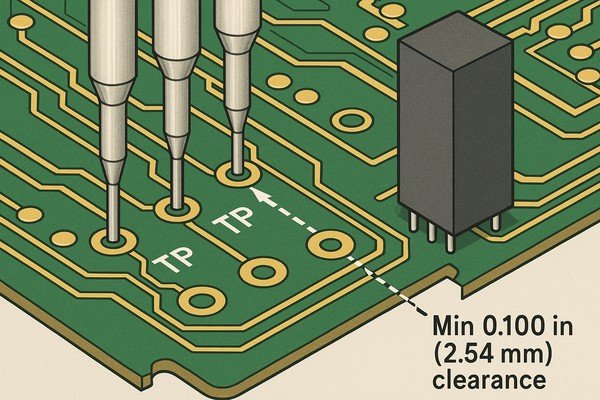
A test fixture operates in three dimensions. The fixture needs space not just for the probe tip, but for the entire probe body and its housing.
The 3D Challenge of Component Clearance in Testing
| Rule | Guideline | Rationale |
|---|---|---|
| Standard Clearance | Maintain 0.100" (2.54mm) clearance between a test point and components up to 0.25" (6.35mm) tall. | Provides enough space for the probe body and housing without physical obstruction. |
| Height-Based Clearance | For components taller than 0.25", add extra clearance. A rule of thumb is to add 0.020" (0.5mm) of clearance for every 0.100" (2.54mm) of component height. | Taller components cast a larger "shadow," requiring the probe to be placed further away to approach the target vertically. |
| Tooling Hole Clearance | Keep a component-free area of at least 0.200" (5.08mm) diameter around all tooling holes. | This area is required for the fixture's mechanical alignment pins to engage without being blocked. |
The Critical Role of Tooling Holes for Fixture Alignment
Place at least two, preferably three, unplated tooling holes diagonally across the board. These are used to align the PCB perfectly within the fixture. Ensure there is a component-free area around these holes so the fixture's alignment pins can engage without being blocked.
Can Vias be Used as Test Points for In-Circuit Testing?
Running out of space on a dense PCB for dedicated test pads? This is a common problem that can leave critical nets untested, creating a blind spot in your quality control and risking field failures.
Yes, vias can absolutely be used as test points for in-circuit testing, and it is a very common practice. However, they must be designed correctly: the via should not be covered by solder mask ("tented"), and its drill hole should be small enough to provide a solid surface for the probe.
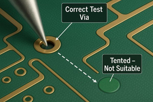
Using vias as test points is an excellent way to save space, but you have to plan for it in your design and be aware of the risks.
Designing a "Testable" Via
| Good Test Point Via | Bad Test Point Via | Why it Matters |
|---|---|---|
| Solder mask opening is at least the size of the via pad. | Tented via (covered with solder mask). | The probe needs to contact a metal surface. Solder mask is an insulator and will block the connection completely. |
| Hole size is small, typically ≤ 0.020" (0.5mm). | Large hole size relative to the pad. | A large hole gives the probe nothing to press against. The probe tip might get stuck or make poor contact with the thin annular ring. |
| Pad size is sufficient, ideally matching a dedicated test pad (~0.040"). | Pad size is minimal (just an annular ring). | A larger pad provides a better target for the probe, increasing the reliability of the connection. |
Associated Risks of Probing Vias
While useful, probing vias isn't without risk. It's a trade-off between accessibility and potential damage.
| Risk Type | Description | Mitigation Strategy |
|---|---|---|
| Mechanical Stress | A sharp, high-pressure probe can fracture the plated barrel of the via, creating an open circuit that may only show up as a field failure later. | Use lower-pressure probes where possible. Avoid using vias as test points for nets that are structurally critical or subject to vibration. |
| Signal Integrity | Probing a via on a high-speed differential pair can introduce an impedance discontinuity, potentially affecting high-frequency test results. | For critical high-speed lines (>1 Gbps), use dedicated test pads placed on short stubs from the main trace rather than probing the via directly. |
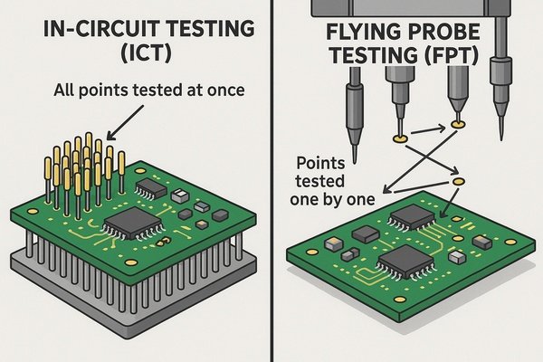
What Are the Differences Between In-Circuit Testing (ICT) and Flying Probe Testing?
You need to test your prototypes, but the cost and lead time for a full bed-of-nails fixture are prohibitive. This leaves you wondering if there's a better way to get the test coverage you need without the massive upfront investment.
The main difference is that In-Circuit Testing (ICT) uses a custom, high-density bed-of-nails fixture to test all points simultaneously, making it extremely fast for high-volume production. Flying Probe Testing (FPT) uses 2-6 robotic probes that move sequentially to test points, requiring no custom fixture, making it ideal for prototypes and low-volume runs.
Choosing between ICT and flying probe testing is a critical decision that depends on your production volume, budget, and time-to-market needs.
Head-to-Head Comparison: ICT vs. Flying Probe
| Feature | In-Circuit Testing (ICT) | Flying Probe Testing (FPT) |
|---|---|---|
| Methodology | Simultaneous contact using a custom bed-of-nails fixture. | Sequential contact using robotic probes. |
| Speed | Extremely fast. Typically 5-10 seconds per board. | Much slower. Typically 1-5 minutes per board. |
| Upfront Cost | Very high. A custom fixture can cost $5,000 - $50,000+. | Very low. No custom fixture cost, only programming time. |
| Flexibility | Inflexible. Any PCB layout change requires a costly fixture modification. | Extremely flexible. A layout change only requires a software update. |
| Power-up Testing | Excellent. Can safely power up the board and perform basic functional checks. | Limited. Can perform some power-up tests, but it's more complex and riskier. |
| Best Use Case | High-volume manufacturing (>5,000 units) with a stable design. | Prototyping & low-volume production (<1,000 units). |
Using a Hybrid Test Strategy for Product Development
Use FPT for initial prototype runs (EVT, DVT) to get detailed test feedback and make design changes quickly. Once the design is stable and you are ramping for mass production (PVT), invest in the ICT fixture. This two-stage approach gives you flexibility early on and speed later.
What Are the Cost Implications of Using a Fine Pitch Test Fixture?
Your PCB is so dense that you're forced to use test points with less than 100-mil spacing. This decision seems necessary, but you're unaware of the hidden costs that can quickly escalate your project's budget.
Using a fine pitch (<100 mil) test fixture significantly increases costs. A 50-mil pitch fixture can cost 2x to 5x more than a standard 100-mil fixture due to more expensive probes, higher precision manufacturing, complex wiring, and increased maintenance requirements.
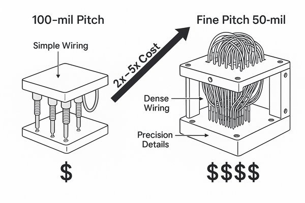
When you move to finer pitches, several factors contribute to a steep rise in cost.
Detailed Cost Breakdown for Fine Pitch Fixtures
| Cost Factor | Standard Pitch (100-mil) | Fine Pitch (50-mil) | Why the Increase? |
|---|---|---|---|
| Test Probes | ~$0.50 - $1.00 per pin | ~$2.00 - $5.00+ per pin | Finer probes require more exotic materials and precision manufacturing to maintain spring force in a smaller form factor. |
| Fixture Manufacturing | Standard CNC drilling tolerances are sufficient. | Requires high-precision drilling (often laser), a more expensive process. | The tolerance for error is much smaller. A slight misalignment will cause failures on a 50-mil grid. |
| Wiring | Often done with automated wire-wrapping machines. | Almost always requires manual, hand-wired connections, which is extremely labor-intensive. | The density of the pins makes automated wiring impossible. |
| Maintenance | Probes are robust and last for 500k-1M cycles. | Probes are more fragile, prone to bending, and wear out faster, leading to higher maintenance costs and downtime. | The smaller physical size makes them less mechanically stable. |
The Hidden Cost: Debugging Fine Pitch Fixtures
When a fine-pitch fixture has a problem—like an internal broken wire or a faulty pin—troubleshooting is a nightmare. The sheer density makes it incredibly difficult to access, diagnose, and repair the issue, leading to extended production downtime that can be even more costly than the fixture itself.
How can I ensure my PCB design is optimized for manufacturing and testing?
You've finalized a brilliant design, but if it can't be built or tested efficiently, it's dead on arrival. Many engineers focus purely on functionality, only to face massive delays and cost overruns when the design hits the factory floor.
To optimize a PCB for manufacturing and testing (DFM/DFT), you must involve your manufacturing partner early, adhere to their specific capabilities, establish clear component placement rules, and implement a comprehensive test point strategy from the very beginning of the design process.

Optimizing your design is a mindset that balances design goals with real-world production realities. The smoothest projects were always the ones where we treated our contract manufacturer (CM) as a partner, not just a vendor.
Step 1: Communicate Early and Often with Your Manufacturer
Before you even finalize your component selection, talk to your intended manufacturer. Ask for their DFM guidelines and design to their "sweet spot," not the absolute minimums. Discuss your layer stack-up with them to ensure the materials are readily available.
Step 2: Implement Design for Assembly (DFA) Principles
Group similar components with the same orientation to speed up the pick-and-place machine. Ensure adequate spacing between components for rework. Place at least three fiducial markers on your board for machine alignment. Also, consider panelization. If your board is part of a larger panel, ensure tooling holes and fiducials are placed on the panel frame (or "breakaway rails") for handling by assembly and test machines.
Step 3: Integrate a Comprehensive Design for Test (DFT) Strategy
Aim for 100% test point coverage, with one test point for every net. Follow the guidelines for pad size, spacing, and clearance. Place all test points on one side of the board. Provide a detailed test point report along with your Gerbers.
What are some common causes of failure in bed-of-nails testing?
You've designed your board, built your fixture, and started production, but now you're getting sporadic test failures. These "ghost" issues are frustrating, kill your production yield, and can be incredibly difficult to diagnose.
Common failures in bed-of-nails testing are often caused by poor contact between the probe and test point due to contamination or misalignment, board flexure from insufficient support, fixture wear-and-tear, and electrostatic discharge (ESD) events.
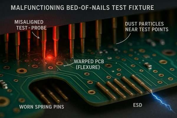
When a board fails ICT, the testing process is just as likely to be the source of the problem as the board itself. Below are the top culprits I've encountered, followed by a summary table.
Failure Cause 1: Poor Probe Contact
This is the number one cause of intermittent failures. Contamination from flux residue, dust, or oils on the PCB test points can create an insulating layer. The tips of the pogo pins can also accumulate this debris, leading to high-resistance connections that cause false failures.
Failure Cause 2: PCB Flexure During Test
If there is a high concentration of test probes in one area of the board with no support on the opposite side, the pressure can cause the PCB to bend. This flexing can cause open circuits at BGA solder balls (pad cratering) or even crack ceramic capacitors.
Failure Cause 3: Fixture and Probe Wear Over Time
Pogo pins are mechanical parts with a finite lifespan, typically rated for 500,000 to 1,000,000 cycles. Over time, the internal spring weakens, reducing contact force. The tips can also become dull or bent, especially on fine-pitch fixtures.
Failure Cause 4: Electrostatic Discharge (ESD) Damage
This is a silent killer. A static discharge from the fixture to the PCB can instantly destroy sensitive components. The cause is often improper material selection for fixture parts or inadequate grounding of the fixture and the operator.
Failure Cause 5: Incorrect Test Program Tolerances
This is a software, not a hardware, problem. The test program might be looking for a resistor value of 1000Ω ±1%, but the resistors on the board are specified at ±5%. This overly tight tolerance will cause perfectly good boards to fail.
| Failure Mode | Common Causes | Solution / Prevention |
|---|---|---|
| Poor Probe Contact | Contamination (flux, dust), oxidized pads, insufficient probe force. | Implement a regular cleaning schedule for probes. Use serrated-tip probes. Ensure proper board surface finish (ENIG/HASL). |
| PCB Flexure | Uneven probe distribution, insufficient board support in the fixture. | Distribute test points evenly. Work with the fixture designer to add support posts opposite high-density probe areas. |
| Fixture/Probe Wear | Probes exceeding their rated lifecycle (500k-1M cycles), bent or damaged probes. | Track the number of cycles on the fixture. Implement a preventative maintenance schedule to replace worn probes. |
| Electrostatic Discharge (ESD) | Improper fixture materials (static-generating plastics), poor grounding. | Build the fixture with ESD-safe materials. Ensure the fixture and operator are properly grounded to the test station at all times. |
| Incorrect Test Tolerances | Test limits in the software are tighter than the component's actual specification. | Review test limits to ensure they account for the specified tolerances of all components on the board. |
Conclusion
Mastering the standards for bed-of-nails testing is not just an academic exercise; it is a fundamental skill for any hardware engineer. From pitch selection to component placement, every decision impacts manufacturability, cost, and reliability.
-
Learn how HASL improves PCB test pad reliability, prevents oxidation, and ensures consistent electrical contact during testing. ↩
-
Learn why ENIG is a top choice for PCB test pads, offering reliable, low-resistance contacts and superior durability compared to other finishes. ↩
-
Learn how OSP works, its pros and cons, and why it may affect test pad reliability in PCB assembly and testing. ↩


