 Skip to content
You've spent weeks on a complex PCB design, only to worry about it failing during fabrication. Warping, uneven traces, and bad yields are common nightmares. What if a simple, often-overlooked feature could drastically improve your board's reliability?
A dummy via is a non-functional plated through-hole added to a PCB to improve manufacturability. Its main purpose is to balance copper distribution for uniform plating and provide mechanical support during drilling, which prevents board warping and ensures a more reliable and higher-yield manufacturing process.
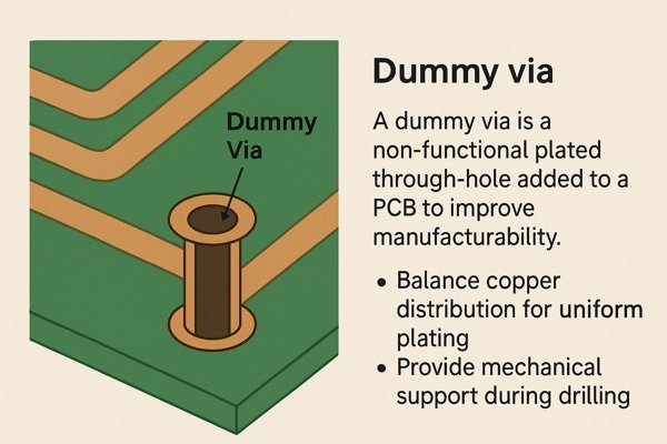
It sounds almost too simple—adding "do-nothing" holes to make a board work better. But as an engineer who has troubleshot manufacturing failures, I can tell you that the impact is profound. I've seen expensive, high-density boards turn into useless, warped pieces of FR-4 simply because of imbalanced copper. These dummy vias are a key tool in our Design for Manufacturability (DFM) toolkit. To use them effectively, we first need to understand how they differ from the standard vias we use every day.
What is the difference between a via and a dummy via?
Are you getting confused by the different types of vias showing up in your layout tool? It's easy to mix up vias that carry signals with ones that are just there for fabrication. Telling them apart is fundamental to creating a robust design.
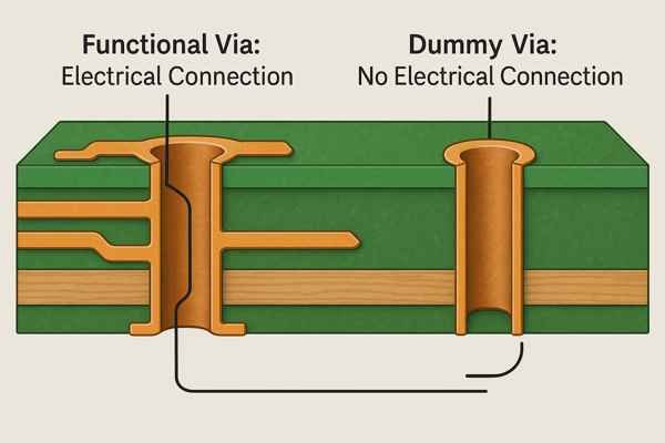
A standard, or functional, via is there to create an electrical path between different layers of your PCB. In contrast, a dummy via is intentionally not connected to any electrical circuit. It's a ghost in the machine, existing only for mechanical and manufacturing purposes.
Functional Role vs. Manufacturing Role
The core of the difference lies in their engineering intent. A functional via is placed by you or your auto-router for one reason only: to complete an electrical circuit. Its location is dictated by the schematic's netlist and the optimal path for routing a signal or power trace.
A dummy via's placement, however, is driven by the physical realities of manufacturing. As the design engineer, you add them deliberately to solve mechanical problems. You place them in areas with low copper density to balance the layer, or in wide-open spaces to give a drill bit extra support. They serve the fabrication house as much as they serve your design.
This table breaks down the essential differences:
| Feature | Functional Via | Dummy Via |
|---|---|---|
| Primary Purpose | Electrical connection between layers | Mechanical support & copper balancing |
| Electrical Connection | Connected to a net (e.g., GND, 5V, Signal) | No net assigned (electrically isolated) |
| Placement Driver | Schematic connectivity and routing needs | DFM rules and physical board layout |
| Impact if Removed | Creates an open circuit (electrical failure) | May lead to manufacturing defects (warp, poor plating) |
How does a dummy via improve PCB manufacturability?
Are you worried that your complex board design will fail during fabrication? Manufacturing yields can be frustratingly unpredictable. The good news is that a simple and strategic addition can significantly improve your chances of a successful production run.
Dummy vias enhance manufacturability primarily in two ways: they create uniform copper density to ensure even plating and prevent warping, and they provide mechanical stability for the drill bit, which results in more accurate hole placement, especially in sparse areas of the board.
Solving the Plating Imbalance Challenge
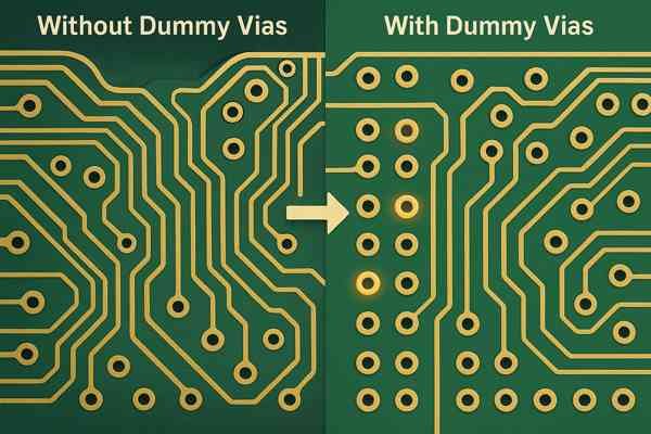
During fabrication, the PCB panel is submerged in an electroplating bath to deposit copper into the via holes. This process relies on electric current. If your board has a large, empty area, that area has low copper density and acts like a current magnet in the bath. It draws a disproportionate amount of current, causing the vias and traces there to become over-plated (too thick). Conversely, dense areas get starved for current, leading to under-plating (too thin). This is a recipe for disaster, with inconsistent impedances and unreliable via barrels. Dummy vias act as "current thieves," strategically placed in sparse areas to draw off some of that excess current, ensuring the entire panel plates at a uniform rate.
Counteracting Thermal Stress and Warpage
A PCB is a composite material, primarily FR-4 laminate and copper. These two materials expand at very different rates when heated, a property known as the Coefficient of Thermal Expansion (CTE)1.
| Material | Typical CTE (\(\text{ppm/}^{\circ}\text{C}\)) |
|---|---|
| Copper | \(\approx 17\) |
| FR-4 (X, Y axes) | \(\approx 14\) |
| FR-4 (Z axis) | \(\approx 70\) (much higher!) |
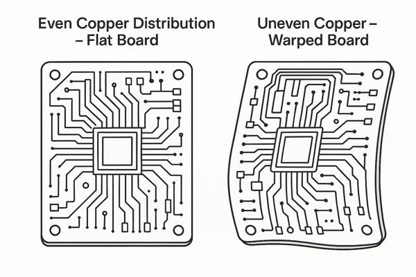
When a board with an imbalanced copper layout is heated during reflow soldering (to over \(200^{\circ}\text{C}\)), the side with more copper expands more, creating immense stress and causing the board to warp. I once had a prototype for a large controller board that came back looking like a potato chip because one layer was a massive ground plane while the opposing layer had only a few traces. Adding a grid of dummy vias and copper hatching on the sparse layer solved it completely.
Providing Mechanical Stability for Drilling
A tiny drill bit (e.g., \(0.2 \text{ mm}\)) is flexible. When it hits the laminate in an open area with no surrounding features, it can deflect slightly upon impact before it starts cutting. This "drill wander" can cause the hole to be off-center, jeopardizing the required minimum annular ring and risking a breakout. Dummy vias provide physical, lateral support to the drill bit, keeping it perfectly aligned as it enters the laminate, ensuring precision.
What is copper balancing and why is it important for PCBs?
Have you ever received a batch of freshly manufactured PCBs, only to find they are noticeably warped or twisted? This frustrating and costly issue often stems from an overlooked design principle. Understanding this principle is the key to preventing it.
Copper balancing is the practice of distributing copper mass as evenly as possible across each individual layer of a PCB and throughout the entire layer stack-up. It is critically important because it ensures uniform plating thickness, prevents the board from warping during assembly, and ultimately improves manufacturing yield and long-term reliability.
The Physics of PCB Warpage
The root cause of warpage is the CTE mismatch between copper and FR-4 laminate. During reflow soldering, when the board temperature rises by over \(200^{\circ}\text{C}\), an imbalanced copper load creates immense internal stress. The side with more copper tries to expand more than the side with less copper, forcing the entire structure to bend and twist. A warped board is a nightmare for assembly; components won't sit flat, and BGA solder joints will be unreliable or fail completely.
Achieving Symmetrical Construction
The goal of copper balancing is to achieve a mechanically symmetrical stack-up. The industry standard IPC-2221B2 (Section 9.1.5) recommends designing your stack-up so that layers are balanced around the center of the board.
| Layer (Top Half) | Pairs With | Layer (Bottom Half) |
|---|---|---|
| Layer 1 (Top) | with | Layer 8 (Bottom) |
| Layer 2 (Inner) | with | Layer 7 (Inner) |
| Layer 3 (Inner) | with | Layer 6 (Inner) |
| Layer 4 (Inner) | with | Layer 5 (Inner) |
Ensuring Uniform Plating Thickness
Beyond warpage, copper balancing is essential for the plating process. Think of the plating current like water pressure. If you have one giant hole in a bucket, all the water rushes out there. If you have many small, evenly spaced holes, the water flows out uniformly. Dummy vias and copper thieving add more "holes" for the plating current to flow through, preventing any one area from being flooded (over-plated) or left dry (under-plated). This ensures every via on your board gets the specified copper thickness for maximum reliability.
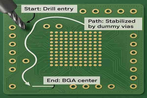
How to use dummy vias for better drill accuracy?
Are you frustrated by misaligned vias, especially in dense footprints like BGAs? Even a slight drill wander can ruin an entire panel of boards. Fortunately, there’s a simple mechanical trick you can use in your layout to ensure drilling precision.
To improve drill accuracy, you should strategically place dummy vias in large, empty sections of your board or around critical footprints. These vias act as mechanical anchors in the laminate, reducing drill bit wander and deflection and ensuring the final drilled holes are precisely aligned with their target pads.
The Mechanics of Drill Wander
A mechanical drill bit used for microvias has a very high aspect ratio (it's long and thin). This makes it inherently flexible. When the bit hits the smooth, unsupported surface of the laminate, it can easily deflect by a few micrometers before it begins to penetrate. This is "drill wander." While this deviation is tiny, it can be enough to violate the minimum annular ring requirement for a pad, which is a critical manufacturing defect according to IPC-A-600. The positional accuracy tolerance for a fabricator might be \(\pm 3 \text{ mils}\) (\(0.076 \text{ mm}\)), and drill wander in a sparse area can eat up that entire budget.
Strategic Placement Guidelines
To be effective, dummy vias for drill support must be placed intelligently. Random placement is not enough.
| Placement Strategy | Rationale | Recommended Practice |
|---|---|---|
| In Large Open Areas | Provides a uniform mechanical surface, preventing the drill from wandering across large spans. | Place vias in a consistent grid, e.g., \(100 \times 100 \text{ mils}\) (\(2.54 \text{ mm}\)). |
| Around Dense Footprints | Stabilizes the drilling area before the machine moves to the critical, high-pin-count component. | Add a "guard ring" or pattern of dummy vias just outside the BGA or connector courtyard. |
| Along Board Edges | Reinforces the edges of the PCB panel, which can be prone to registration issues and deformation. | Place a line of dummy vias inside the board edge, parallel to the outline. |
By implementing these strategies, you are proactively helping your fabricator stay well within their process tolerances, leading to higher yields and more reliable boards.
What are thermal vias and how are they different from dummy vias?
Is your power converter IC or high-current MOSFET overheating despite being placed on a large ground plane? You might be missing a critical thermal pathway. It's important not to confuse the vias needed for this job with the purely mechanical dummy vias.
Thermal vias are designed specifically to transfer heat away from a hot component down to a larger copper plane, which acts as a heat sink. Unlike dummy vias, which are electrically isolated and exist for manufacturing purposes, a thermal via is electrically connected to the component's thermal pad.
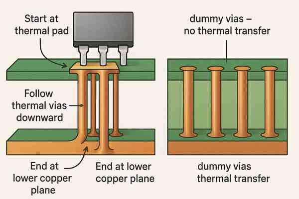
Primary Function: Heat vs. Manufacturability
The purpose of a thermal via3 is to create a low-resistance path for thermal energy. It's a heat pipe. The purpose of a dummy via is to solve mechanical manufacturing problems. It's a structural support. This fundamental difference in intent dictates their design.
Design and Construction Differences
You design a thermal via to maximize heat transfer. This means:
- Placement: Placed in an array directly under a component's thermal pad.
- Size: Often larger than signal vias (\(0.3 \text{ mm to } 0.5 \text{ mm}\) diameter) to increase the cross-sectional area for heat flow.
- Filling: For high-power applications, they are often filled with thermally conductive epoxy. This epoxy can have a thermal conductivity of \(1-10 \text{ W/m}\cdot\text{K}\), vastly superior to the \(\approx 0.25 \text{ W/m}\cdot\text{K}\) of the trapped air in an open via.
Dummy vias, by contrast, are designed for uniformity and low cost. They are typically a standard small via size (e.g., \(0.2 \text{ mm}\) hole) and are left unfilled.
| Feature | Thermal Via | Dummy Via |
|---|---|---|
| Primary Function | Heat dissipation | Manufacturability (copper balance, drill support) |
| Electrical Connection | Yes (connected to thermal pad/plane) | No (electrically isolated) |
| Typical Location | Directly under a heat-generating component | In sparse, open areas of the board |
| Design Goal | Minimize thermal resistance | Achieve uniform copper density and mechanical stability |
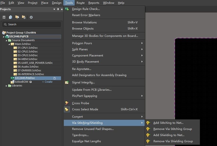
How do you add dummy vias in Altium Designer?
Do you want to add dummy vias to your PCB design but dread the thought of placing hundreds of them one by one? Manually adding them is not only incredibly tedious but also prone to errors. The good news is you can automate this entire process in Altium Designer.
In Altium Designer, the most efficient way to add dummy vias is by using the Via Stitching tool. The trick is to configure the tool to stitch to a "No Net" assignment instead of a specific electrical net like GND. This will automatically fill a selected polygon or the entire board with electrically isolated dummy vias.
Step-by-Step Implementation and Settings
The process is straightforward when you know which settings to use in the Tools > Via Stitching/Shielding dialog.
| Setting | Recommended Value | Reason |
|---|---|---|
| Stitching Net | No Net | This is the key step that makes them "dummy" vias, ensuring they are electrically isolated. |
| Grid | \(50-100 \text{ mils}\) (\(1.27-2.54 \text{ mm}\)) | Defines the spacing. A sparser grid is usually sufficient and prevents mechanical weakening. |
| Via Style/Template | A standard via from your design | Avoids adding new drill sizes, which keeps fabrication costs down. Use a common size like \(0.2\text{mm}/0.4\text{mm}\). |
| Constrain to Polygon | Checked (if using a polygon) | Gives you precise control to add vias only in the sparse areas where they are needed for copper balancing. |
Pro-Tips for Management
- Create a Dedicated Design Rule: I always create a specific clearance rule for my dummy vias and put them in their own class ("Dummy_Vias"). This allows me to set their clearance to other objects independently and makes them easy to manage.
- Toggle Visibility: In the View Configuration panel, you can toggle the visibility of "No Net" vias to clean up your display when you are focused on routing active signals.
What is via stitching and how does it relate to dummy vias?
You may have heard the term "via stitching" in the context of improving EMI performance or ensuring good ground connections. How does this relate to the dummy vias we've been discussing? Are they the same thing?
Via stitching is a design technique used to connect large copper areas (like ground or power planes) on different layers using an array of vias. Its primary purpose is electrical: to ensure a low-impedance path and create a solid ground return path, which is critical for signal integrity and EMI control. It is related to dummy vias because the same software tool used to perform via stitching is often used to create dummy vias. The key difference lies in the net assignment.
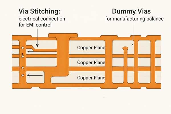
The Electrical Goal of Via Stitching
The engineering intent behind via stitching is to create a robust electrical connection between same-net planes. For ground planes, this array of vias effectively creates a Faraday cage, helping to shield sensitive circuits from electromagnetic interference (EMI)4. It also provides many short, low-inductance paths for high-speed signal currents to return to their source, which is absolutely critical for maintaining good signal integrity5. Every via in the stitch is functional and carries current.
The Mechanical Goal of Dummy Vias
The goal of adding dummy vias is, as we've discussed, purely mechanical and manufacturing-related. They are there to balance copper density and provide drill support. They are intentionally designed not to carry any current. They are passive structural elements.
It's a common point of confusion because the process in your EDA software looks identical. You select an area and fill it with a grid of vias. However, the engineering outcome is completely different based on one setting:
| Feature | Via Stitching | Dummy Via Creation |
|---|---|---|
| Purpose | Electrical (Low impedance, EMI shield) | Mechanical (Copper balance, drill support) |
| Net Assignment | Assigned to a specific net (e.g., GND) | Assigned to No Net |
| Software Tool | Typically the "Via Stitching" tool | Typically the "Via Stitching" tool |
| Engineering Intent | Create a functional electrical structure | Create a non-functional mechanical structure |
Are there DFM (Design for Manufacturability) rules for placing dummy vias?
You're ready to add dummy vias to your design for better manufacturability, but you're wondering if you can just place them anywhere. To avoid creating new problems while solving others, you should follow a few key Design for Manufacturability (DFM) rules.
Yes, there are established DFM guidelines for placing dummy vias. The most important rules are to maintain adequate clearance from all active copper features to prevent shorts, to use a standard and manufacturable via size, and to maintain a consistent grid pattern that doesn't mechanically weaken the board.
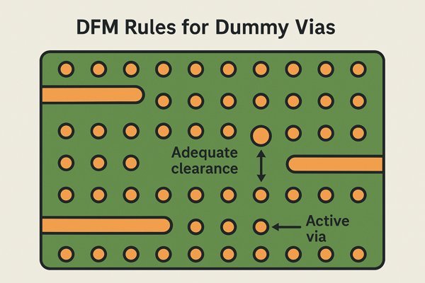
To ensure success, treat dummy vias with the same care as functional components of your design by following these rules:
| DFM Rule | Guideline | Why It's Important |
|---|---|---|
| Maintain Electrical Clearance | Keep a minimum of \(8-10 \text{ mils}\) (\(0.2-0.254 \text{ mm}\)) between dummy vias and any active copper. | Prevents accidental short circuits caused by normal manufacturing tolerances in drilling and etching. |
| Use a Standard Via Size | Use a common via size already in your design (e.g., \(0.2 \text{ mm}\) drill / \(0.4 \text{ mm}\) pad). | Avoids adding unique drill sizes, which increases fabrication cost and complexity. |
| Ensure a Robust Annular Ring | Design the via pad to guarantee at least a \(1 \text{ mil}\) (\(0.025 \text{ mm}\)) annular ring per IPC-A-600 Class 2. | A sufficient annular ring is critical for a reliable via connection and prevents pad breakout during drilling. |
| Control Placement Density | Use a consistent grid, e.g., \(50-100 \text{ mils}\) (\(1.27-2.54 \text{ mm}\)). Avoid overly dense patterns. | Prevents the "perforation effect," where too many holes weaken the laminate and create a potential breaking point. |
What is the impact of dummy vias on signal integrity?
You're a diligent engineer, and while you want the manufacturing benefits of dummy vias, you're rightfully concerned about any potential negative impact on your high-speed signals. Could these non-functional vias cause unintended problems?
When placed correctly with proper clearances, the impact of dummy vias on signal integrity is negligible for the vast majority of designs. Because they are electrically isolated ("floating"), they do not directly interact with signal traces or provide a path for current to flow.
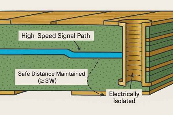
Capacitive Coupling: A Minor Concern
Any two conductors placed near each other will have some parasitic capacitance6. A dummy via placed very close to a high-speed trace could, in theory, capacitively couple to it and slightly alter the trace's impedance. However, the effect is extremely small. Standard DFM clearance rules of \(8-10 \text{ mils}\) (\(0.2 \text{ mm} - 0.254 \text{ mm}\)) create enough distance to render this effect insignificant for all but the most demanding multi-gigabit applications.
Return Path Discontinuity: The Real (but Small) Risk
This is a more valid concern. Every via that passes through a solid ground plane requires a clearance hole (an anti-pad) in that plane. This anti-pad creates a small void. If a high-speed signal's return current encounters this void, it must flow around it, which creates a small impedance bump. However, it's important to compare the impact of a dummy via to a signal via:
| Via Type | Impact on Return Path | Reason |
|---|---|---|
| Signal Via | High | The signal current itself changes layers, forcing the return current to find a new path, often through a distant stitching via. This can create a large current loop. |
| Dummy Via | Very Low | The signal trace remains on its original layer. The return current merely has to navigate around a tiny obstacle (the anti-pad), causing a negligible deviation. |
For a well-designed board, the manufacturing benefits of copper balancing almost always outweigh this very small and manageable signal integrity risk.
Can dummy vias cause problems in a PCB design?
While dummy vias are a powerful tool for improving manufacturability, you're right to be cautious. Like any design feature, if they are implemented improperly, they can certainly cause problems. The key is to use them wisely.
Yes, dummy vias can cause problems in a PCB design if they are not implemented according to DFM guidelines. The most common issues are creating accidental electrical shorts if placed too close to active copper, or mechanically weakening the board if they are placed too densely.
These problems are not inherent flaws of the technique but are results of poor implementation. Here is how to avoid them:
| Potential Problem | Root Cause | Recommended Solution |
|---|---|---|
| Electrical Shorts | Insufficient clearance between dummy via pad and adjacent active copper (traces, pads). | Enforce a strict via-to-copper clearance rule of at least \(8-10 \text{ mils}\) (\(0.2-0.254 \text{ mm}\)) in your DRC. |
| Mechanical Weakness | Placing vias too densely, creating a "perforation effect" that weakens the board laminate. | Use a reasonable grid spacing, like \(100 \text{ mils}\) (\(2.54 \text{ mm}\)), and avoid creating long, straight lines of vias. |
| Acid Traps | An older concern where acute angles in copper trap etching chemicals, causing over-etching. | Maintain proper spacing between vias. Modern fab processes and DRCs largely mitigate this risk. |
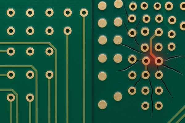
How does the plating process affect via reliability?
You've designed your vias perfectly, but what happens during manufacturing? The reliability of every single via on your board, whether functional or dummy, is heavily dependent on the quality of the copper plating process.
The electroplating process is absolutely critical for via reliability. An inconsistent or poorly controlled process results in thin or uneven copper plating inside the via barrel. This thin plating is highly susceptible to cracking under the thermal stress of assembly or normal operation, leading to intermittent or total open circuits.
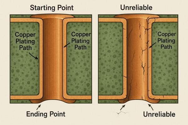
The Critical Role of the Aspect Ratio
The biggest challenge for the plating process is the via's Aspect Ratio, calculated as:
\(\text{Aspect Ratio} = \frac{\text{PCB Thickness}}{\text{Via Drill Diameter}}\)
A \(0.2 \text{ mm}\) via in a \(1.6 \text{ mm}\) PCB has an \(8:1\) ratio. As this ratio increases (generally \(>10:1\)), it becomes exponentially harder for the plating solution's chemical ions to flow deep into the narrow hole. This can lead to ion depletion in the center of the barrel, resulting in much thinner copper plating there compared to the ends.
IPC Standards for Plating Thickness
The IPC-6012E7 standard defines the minimum requirements for via plating to ensure reliability against thermal and mechanical stress.
| IPC Class | Typical Application | Minimum Plating Thickness (Average) |
|---|---|---|
| Class 2 | Standard Commercial, Industrial | \(20 \mu\text{m}\) (\(0.79 \text{ mils}\)) |
| Class 3 | High Reliability (Medical, Aerospace) | \(25 \mu\text{m}\) (\(0.98 \text{ mils}\)) |
A via with plating thinner than this cannot withstand the Z-axis expansion stress during reflow and is a ticking time bomb for failure. Dummy vias help ensure these minimums are met everywhere on the board.
What are via-in-pad and filled vias?
As you deal with increasingly dense components like BGAs, you'll encounter advanced via technologies like "via-in-pad." How does this technique work, and how does it relate to the other via types we've discussed?
Via-in-pad is a manufacturing technique where a via is placed directly inside the surface-mount pad of a component. To make the pad solderable, the via hole is often filled with conductive or non-conductive epoxy and then plated over with copper, creating a flat, reliable surface known as a "capped via."
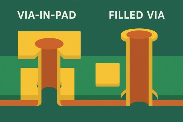
The Challenge: High-Density Fanout
With modern fine-pitch BGAs (e.g., \(0.5 \text{ mm}\) pitch or less), there is physically no room between the pads to run a traditional "dog bone" fanout, where a short trace connects the pad to a nearby via. The only way to escape the signal from an inner pin is to go straight down.
The Solution: Via-in-Pad Plated Over (VIPPO)
The VIPPO process is a multi-step solution that adds cost but enables high-density design. If this process isn't done, the open hole in the pad will wick solder away during reflow, creating a failed joint.
| Process Step | Engineering Purpose |
|---|---|
| Step 1: Drill Create the via hole in the center of the BGA pad. | Prevents solder from wicking down the via barrel. |
| Step 2: Fill Fill the hole completely with a specialized epoxy (non-conductive is standard). | Prevents solder from wicking down the via barrel. |
| Step 3: Planarize Grind the surface so the filled epoxy is perfectly flush with the copper pad. | Creates a flat surface for the final plating step. |
| Step 4: Cap Plate copper over the entire pad, "capping" the filled via. | Provides a smooth, reliable, and fully solderable surface for the BGA ball. |
This final table summarizes how all these via technologies fit together:
| Feature | Standard Via | Dummy Via | Thermal Via | Via-in-Pad (VIPPO) |
|---|---|---|---|---|
| Function | Electrical Routing | Manufacturability | Thermal Transfer | High-Density Routing |
| Net Assignment | Yes | No | Yes | Yes |
| Location | Next to pad | Sparse board areas | Under thermal pad | Inside component pad |
| Primary Cost Driver | Standard | Negligible | Size / Filling | Multi-step filling/capping process |
Conclusion
In short, dummy vias are a simple yet powerful DFM tool. They balance copper, improve drill accuracy, and ensure your board is manufactured reliably, preventing costly issues like warping and bad plating.
-
Understanding CTE is crucial for preventing warpage in PCBs; learn more about its impact on design. ↩
-
Exploring IPC-2221B helps you grasp industry standards for PCB stack-up, essential for achieving mechanical symmetry. ↩
-
Understanding thermal vias is crucial for effective heat management in electronic designs. Explore this link to learn more about their function and design. ↩
-
Understanding EMI is crucial for designing circuits that are resilient to interference, ensuring better performance and reliability. ↩
-
Maintaining signal integrity is vital for high-speed circuits; explore techniques to enhance performance and reduce errors. ↩
-
Understanding parasitic capacitance is crucial for optimizing circuit performance and minimizing signal integrity issues. ↩
-
The IPC-6012E standard is vital for ensuring PCB reliability. Learn more about these standards to enhance your PCB manufacturing knowledge. ↩


