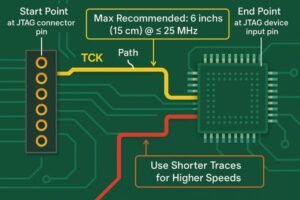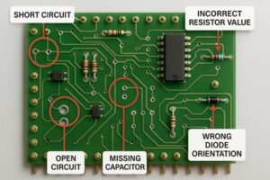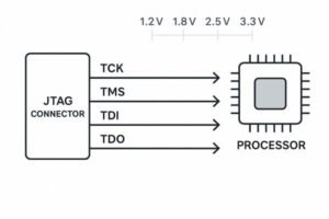
A schematic diagram is a designed circuit representation that shows the functionality of inner circuits and the principle of the connection between various electronic components on a circuit board.It uses standardized symbols to depict components and their connections. Schematics simplify complex circuits, allowing you to visualize how the circuit functions and troubleshoot any issues that may arise.
What is the relationship between schematic, PCB, and PCB Layout?

Schematic

PCB

PCB Layout
A schematic diagram is a graphical representation of the circuit's functionality, illustrating the connections between various components on a circuit board. PCB (Printed Circuit Board) is the physical board that hosts the electronic components and their interconnecting circuitry. PCB Layout is the practical implementation of the functions shown in the schematic on the actual circuit board. From the design process perspective, schematic diagrams and PCB Layouts are conducted sequentially. Their effective integration ensures a smooth transition from theoretical design to actual manufacturing, ultimately impacting the performance and reliability of the final product.
What are the basic elements that make up a schematic diagram?

A schematic diagram is composed of several fundamental elements, each serving a specific function in illustrating the electronic circuit. The basic elements include:
- Symbols for Components: Standardized symbols represent various electronic components such as resistors, capacitors, diodes, transistors, and integrated circuits. These symbols include both pin numbers and reference designators (e.g., R1 for the first resistor, U1 for the first integrated circuit) to uniquely identify each component and specify pin connections.
- Connections (Nets): Lines that represent electrical connections between components. These lines indicate how components are electrically linked.
- Power and Ground Symbols: Symbols representing power supply connections and ground connections, ensuring that the schematic shows how the circuit is powered.
- Labels and Annotations: Text elements that provide specific information related to individual components or connections, such as signal names, voltage levels, component values, and functional descriptions. These labels are placed close to the relevant parts of the schematic to aid in quick identification and understanding.
- Buses: Groups of parallel lines representing multiple electrical connections that are bundled together, used for simplifying the schematic when dealing with multiple connections.
- Connection Dots (Junctions): Small dots where lines intersect, indicating electrical connections between the intersecting lines.
- Notes and Legends: Text elements that offer additional context or instructions applicable to the entire schematic. This includes explanatory notes about the circuit design, assembly or testing instructions, and a legend explaining the symbols or abbreviations used. These are typically found in the margins or at the bottom of the schematic.
- Title Block: A section of the schematic that includes important information such as the title of the diagram, the date, the designer's name, and other relevant metadata.
What are the standards for schematic symbols?
Standards for schematic symbols ensure consistency and clarity in electrical and electronic diagrams. These standards are established by various international organizations to provide uniformity in the representation of components. Here are some of the primary standards for schematic symbols:
- IEEE Std 315 / ANSI Y32: Known as the "Graphic Symbols for Electrical and Electronics Diagrams," this standard provides comprehensive symbols for electrical and electronic components and is widely used in North America. It was originally published as ANSI Y32 and later adopted and revised by the IEEE as IEEE Std 315.
- IEC 60617: Maintained by the International Electrotechnical Commission (IEC), this standard is commonly used in Europe and other regions. It provides a standardized set of graphical symbols for electrical diagrams.
- ISO 14617: Provided by the International Organization for Standardization (ISO), this standard includes graphical symbols for diagrams used globally and covers a broad range of symbols for various industries.
- JIS C 0617: Provided by the Japanese Industrial Standards (JIS), this standard aligns closely with the IEC standards and is used in Japan for electrical and electronic diagrams.
- DIN 40700 Series: Provided by the Deutsches Institut für Normung (DIN), this series covers graphical symbols for electrical engineering and electronics in Germany.
What are the different schematic symbols?
Schematic symbols are graphical representations used to denote various electronic components in circuit diagrams. These symbols are standardized to ensure clarity and consistency in electronic design and communication. Here is a comprehensive list of various schematic symbols and their detailed explanations:
Resistors

- Fixed Resistor: Represented by a zigzag line (standard in the U.S.) or a rectangle (commonly used internationally). This resistor offers a constant, unchanging resistance value, which limits the flow of electric current and helps control voltage and current within the circuit. Its resistance is measured in ohms (Ω). Common applications include voltage dividers, current limiting, and setting bias points in transistor circuits.
- Variable Resistor (Rheostat): Represented by a zigzag line with an arrow intersecting it. A rheostat typically has two terminals: one connected to one end of the resistive element and the other to the wiper, which moves along the resistive path to adjust the resistance. Unlike a potentiometer (which has three terminals), a rheostat primarily controls current, making it useful for applications like tuning and adjusting current in lighting dimmers, motor speed controls, and heaters.
- Potentiometer: Represented by a zigzag line with an arrow intersecting across it. A potentiometer has three terminals: two on either end of a resistive element and a third connected to a wiper that moves along the resistive path. It functions as a variable voltage divider, making it ideal for adjustable controls like volume or brightness knobs.
- Trimmer Resistor: A small variable resistor designed for occasional adjustment, represented with a zigzag line and an arrow intersecting at an angle. This is a small, variable resistor used for infrequent or fine-tuning adjustments. Once set, it's usually left as-is, and it’s found in calibration settings where precise resistance is crucial.
- Negative Temperature Coefficient (NTC) Thermistor: An NTC thermistor exhibits a decrease in resistance as temperature increases. The standard symbol is a rectangle (representing a resistor) with a diagonal line intersecting it, often accompanied by a downward arrow or the marking “-t°” to denote the negative temperature coefficient. This type is commonly used for temperature measurement, inrush current limiting to prevent power surges, and over-temperature protection in sensitive circuits.
- Positive Temperature Coefficient (PTC) Thermistor: A PTC thermistor displays an increase in resistance as temperature rises. Its symbol resembles that of a resistor with a diagonal line, typically marked with an upward arrow or the notation “+t°” to indicate the positive temperature coefficient. PTC thermistors are frequently applied in overcurrent protection, self-resetting fuses, degaussing circuits for CRT displays, and as heating elements in certain applications.
- Light Dependent Resistor (LDR): An LDR, or photoresistor, has a resistance that decreases with increased light exposure. The symbol consists of a rectangle or zigzag line with arrows pointing toward it, indicating its sensitivity to light. It has high resistance in the dark, which lowers when exposed to light, making it ideal for light-detecting circuits. Common uses include automatic lighting systems (e.g., street lights), ambient light sensors in devices, and camera light meters.
Capacitors

- Non-Polarized Capacitor: Two parallel lines. This symbol represents a capacitor that stores electrical energy without a specific polarity, meaning it can be connected in any direction. Used for coupling and decoupling applications, filtering, and timing circuits.
- Polarized Capacitor: One curved and one straight line. This symbol indicates a capacitor with a specific polarity, meaning it must be connected in a particular direction. The straight line typically represents the positive terminal. Used in power supply circuits for smoothing and filtering.
- Variable Capacitor: Two parallel lines with an arrow intersecting at an angle. This symbol represents a capacitor whose capacitance can be adjusted. Used in radio frequency (RF) tuning circuits.
Inductors

- Inductor: Series of loops or a coiled line. This symbol represents a component that stores energy in a magnetic field when electrical current passes through it. Used in filters, transformers, and energy storage applications.
- Iron Core Inductor: Coiled line with parallel lines through the center. This symbol represents an inductor with an iron core, which increases its inductance. Used in power supplies and radio-frequency applications.
- Variable Inductor: A variable inductor is an inductor whose inductance can be adjusted by changing the position of its core or the spacing between coils. Its standard symbol is a coil with an arrow diagonally crossing it, signifying the ability to vary the inductance. Variable inductors are useful in tuning circuits to adjust frequency response and in applications where precise control of inductance is required. They are commonly found in radio frequency (RF) circuits, oscillators, and filter circuits where fine-tuning is essential to achieve the desired signal characteristics.
Diodes

- Standard Diode: A triangle pointing to a line. This symbol indicates a component that allows current to flow in one direction only, used for rectification. Commonly found in power supplies and signal demodulation.
- LED (Light Emitting Diode): A diode symbol with two arrows pointing away, indicating a diode that emits light when current flows through it. Used in indicators and display systems.
- Photodiode: A diode symbol with arrows pointing towards it, indicating a diode that generates current when exposed to light. Used in light detection and solar cells.
- Schottky Diode: A standard diode symbol with an added ‘S’ or a distinct line, representing a diode with a low forward voltage drop, used in high-speed switching applications. Found in power rectifiers and RF applications.
- Zener Diode: A diode symbol with bent edges at the end of the line, indicating a diode that allows current to flow in the reverse direction when a specific reverse voltage is reached, used for voltage regulation. Used in voltage reference and protection circuits.
- Varactor Diode: Diode symbol with a line and arrow pointing to a capacitor symbol, indicating a diode whose capacitance varies with the applied voltage, used in tuning circuits. Found in frequency modulation and tuning circuits.
Transistors

- NPN Transistor (NPN Bipolar Junction Transistor): An NPN transistor is a bipolar junction transistor (BJT) that uses both electrons and holes as charge carriers, with current flowing from the collector to the emitter when a small current is applied to the base. Its symbol consists of three terminals: collector, emitter, and base, with an arrow on the emitter pointing outward to indicate the direction of current flow. NPN transistors are widely used in amplification and switching applications, including signal amplification, digital logic circuits, and motor control..
- PNP Transistor (PNP Bipolar Junction Transistor): A PNP transistor is a type of BJT where current flows from the emitter to the collector when a small current flows from the emitter to the base. The symbol is similar to an NPN transistor but with the arrow on the emitter pointing inward. PNP transistors are commonly used for switching and amplifying signals and are typically found in low-power applications, analog circuits, and complementary pairs with NPN transistors in push-pull amplifier configurations.
- JFET-N (N-Channel Junction Field-Effect Transistor): An N-channel JFET is a type of field-effect transistor that controls current flow using an electric field applied to the gate terminal. Its symbol consists of three terminals: drain, source, and gate, with an arrow on the gate indicating the flow of electrons. JFET-N transistors are typically used in analog circuits for signal amplification and are favored in applications requiring high input impedance, such as audio amplifiers and impedance matching circuits.
- JFET-P (P-Channel Junction Field-Effect Transistor): A P-channel JFET operates similarly to an N-channel JFET but has opposite polarity. Current flows from the source to the drain when a reverse bias is applied to the gate. The symbol includes an arrow on the gate pointing inward, indicating the P-channel. JFET-P transistors are also used in analog applications, such as signal amplification and impedance matching, especially where complementary transistor pairs are required.
- NMOSFET (N-Channel Metal-Oxide-Semiconductor Field-Effect Transistor): An NMOSFET uses an electric field to control current flow between the drain and source terminals, with an arrow pointing outward in the symbol to indicate the N-channel. NMOSFETs are commonly used in power management, high-speed switching, and digital circuits due to their fast switching speeds and low on-resistance, making them ideal for switching applications in power supplies and microprocessors.
- PMOSFET (P-Channel Metal-Oxide-Semiconductor Field-Effect Transistor): A PMOSFET operates similarly to an NMOSFET but has an opposite polarity, with the symbol’s arrow pointing inward. Current flows from the source to the drain when positive voltage is applied to the source relative to the gate. PMOSFETs are used in power management and low-power switching and are commonly paired with NMOSFETs in CMOS circuits for efficient digital design.
Integrated Circuits (ICs)
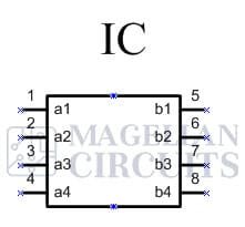
- IC: Rectangle with multiple pins, each labeled with its specific function (e.g., Vcc, GND, Input, Output). This symbol indicates a complex component that integrates multiple electronic functions into a single package, such as amplifiers, microcontrollers, and processors. Used in virtually all modern electronic devices.
Switches

- SPST (Single Pole Single Throw): An SPST switch has one input terminal (pole) and one output terminal (throw), allowing a simple on/off function. This switch type either connects or disconnects a single circuit path. It is widely used for basic on/off controls, such as turning lights or small appliances on and off.
- SPDT (Single Pole Double Throw): An SPDT switch has one input terminal (pole) and two output terminals (throws). It can connect the input to either of the two outputs, allowing for switching between two circuits. SPDT switches are commonly used in applications that require selecting between two options, such as switching between two power sources or toggling between two different signal paths.
- DPST (Double Pole Single Throw): A DPST switch has two input terminals (poles) and two corresponding output terminals (throws), enabling it to control two separate circuits simultaneously. Both circuits are either connected or disconnected at the same time, making this switch ideal for applications where two circuits need to be controlled with a single on/off action, such as controlling both the live and neutral wires in AC power circuits.
- DPDT (Double Pole Double Throw): A DPDT switch has two input terminals (poles) and four output terminals (throws), allowing each input to connect to one of two outputs. This configuration provides switching between two pairs of circuits, functioning as two SPDT switches combined. DPDT switches are used in applications requiring a change in polarity or direction, such as reversing the direction of a motor or selecting between two signal paths.
Power Sources

- Battery: Series of short and long lines, indicating the positive and negative terminals of a battery, which provides a DC voltage supply. Used as a portable power source.
- DC Power Supply: Line with a positive and negative symbol, indicating a direct current supply. Used to provide a constant DC voltage.
- AC Power Supply: Sine wave symbol or circle with a tilde (~), indicating an alternating current supply. Used to provide a constant AC voltage.
Voltage Nodes

- Ground (GND): Set of three descending lines or a triangle pointing downward, indicating a common return path for electric current. Essential for circuit stability and safety.
- Positive Voltage: Line with a plus sign (+) or labeled as Vcc, indicating a positive voltage node. Used as a reference point for positive voltage.
- Negative Voltage: Line with a minus sign (-) or labeled as Vee, indicating a negative voltage node. Used as a reference point for negative voltage.
Connectors
- Connectors are components that join parts of a circuit, enabling secure transfer of signals, data, or power. They come in various types, like wire-to-wire, wire-to-board, and board-to-board, each designed for specific applications. Specialized connectors such as USB, Ethernet, and audio/video provide reliable connections tailored to data, power, and signal needs in electronic devices. These are examples of connectors:

Relays
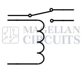
- Relay: Coil and switch combination, indicating an electrically operated switch used to control a high-power circuit with a low-power signal. Used in automation and control systems.
Op-Amps (Operational Amplifiers)
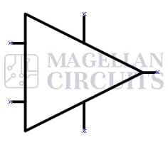
- Op-Amp: A triangle with inputs and outputs labeled, indicating an amplifier with high gain, used in various signal processing applications. Used in amplifiers, filters, and oscillators.
Crystals, Oscillators, and Resonators

- Crystal: A crystal is an electronic component made from quartz or other piezoelectric materials, which vibrate at a precise frequency when subjected to an electric field. It provides a stable oscillation frequency, essential for timing and synchronization in circuits. Unlike an oscillator, a crystal alone does not generate an oscillating signal; it requires an external circuit to function as a complete frequency source. Crystals are commonly used in applications requiring precise timing, such as microcontrollers, clocks, and communication devices.
- Oscillator: An oscillator is an electronic circuit or device that generates a continuous, periodic signal, usually in the form of a sine or square wave. It typically incorporates a crystal, inductor-capacitor (LC) circuit, or resistor-capacitor (RC) network to stabilize its frequency. The main difference between a crystal and an oscillator is that an oscillator is a complete circuit that actively produces an oscillating signal, while a crystal provides the stable frequency but requires additional circuitry to oscillate. Additionally, an oscillator requires a DC power supply to operate, as it is an active device that needs power to amplify and sustain the oscillations. Oscillators are widely used in clock generation, radio frequency (RF) communication, and signal processing applications.
- Resonator: A resonator is a component that generates a specific resonant frequency, similar to a crystal, but often with lower accuracy and stability. Resonators are typically made from ceramic materials and are used in circuits where a stable, but less precise, frequency is sufficient. Common applications include timing in microcontrollers, filters, and simple clock circuits where high precision is not critical.
Transformers
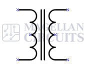
- Transformer: A transformer is an electrical device that transfers energy between two or more circuits through electromagnetic induction. It consists of primary and secondary windings wrapped around a magnetic core. When alternating current (AC) flows through the primary winding, it creates a changing magnetic field that induces a voltage in the secondary winding. Transformers are essential for stepping up (increasing) or stepping down (decreasing) voltage levels, making them crucial for power distribution and voltage regulation in various applications.
Antennas
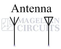
- Antenna: An antenna is an electrical device that transmits and receives electromagnetic waves, enabling wireless communication. It converts electrical signals into radio waves (transmitting) or radio waves into electrical signals (receiving). Antennas come in various types and shapes, designed to operate at specific frequencies and with particular radiation patterns. They are widely used in applications such as radio broadcasting, television, mobile phones, Wi-Fi networks, and satellite communication.
Motors
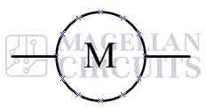
- Motor: A motor is an electromechanical device that converts electrical energy into mechanical energy, creating rotational or linear motion. Motors are essential components in countless applications, from household appliances and industrial machinery to vehicles and robotics. They come in various types, each designed to operate with specific power sources and motion requirements.
Speakers and Buzzers

- Speaker: A speaker is an electroacoustic device that converts electrical signals into sound waves, allowing audio playback. It operates by using a voice coil that moves in response to an audio signal, causing a diaphragm to vibrate and create sound. Speakers vary in size and design to accommodate different frequencies and audio quality requirements. They are widely used in consumer electronics, such as smartphones, televisions, home audio systems, and public address systems.
- Buzzer: A buzzer is an electronic device that produces a single-tone sound or beep when activated by an electrical signal. Buzzers are often used as alert or notification devices and can be either piezoelectric or magnetic. Piezo buzzers create sound by vibrating a piezoelectric disc, while magnetic buzzers use an electromagnet to produce sound. They are widely used in alarms, timers, and appliances where sound-based alerts are needed.
Microphones

- Microphone: A microphone is an electroacoustic device that converts sound waves into electrical signals, allowing audio to be recorded or transmitted. It works by capturing sound vibrations through a diaphragm, which moves in response to sound pressure and generates a corresponding electrical signal. Microphones are used in various applications, including telecommunication, broadcasting, audio recording, and voice recognition systems.
Photoelectric Devices

- Photodiode: A photodiode is a light-sensitive semiconductor device that converts light into an electrical current. When exposed to light, it generates a small current proportional to the intensity of the light, which can be used in sensing and measuring applications. Photodiodes operate primarily in reverse bias, allowing them to respond quickly to changes in light levels. They are widely used in optical communication, light detection, and medical devices such as pulse oximeters.
- Phototransistor: A phototransistor is a light-sensitive transistor that uses light to control current flow, acting as both a photodetector and an amplifier. When exposed to light, the phototransistor generates a base current, which amplifies the current flow between the collector and emitter. Phototransistors are more sensitive than photodiodes and are used in applications like light sensing, object detection, and optical communication systems.
- Solar Cell: A solar cell, also known as a photovoltaic cell, is a semiconductor device that converts sunlight directly into electrical energy. When exposed to sunlight, the solar cell generates a flow of electrons through the photovoltaic effect, producing DC electricity. Solar cells are combined in arrays to form solar panels and are widely used in renewable energy systems, calculators, satellites, and remote power applications.
Protective Devices

- Fuse: A fuse is a current-sensitive protection device that interrupts a circuit by melting a metal wire or strip when the current exceeds a safe level. This breaking of the circuit prevents damage to components and protects against overheating and fire hazards. Fuses are widely used in consumer electronics, automotive systems, and industrial applications for overcurrent protection.
- MOV (Metal Oxide Varistor): An MOV is a voltage-dependent resistor that provides protection by rapidly reducing its resistance when voltage spikes exceed a certain threshold. By diverting excess current, it safeguards sensitive components from overvoltage conditions. MOVs are commonly used in power supplies, surge protectors, and household appliances to prevent damage from power surges and lightning strikes.
- TVS (Transient Voltage Suppression) Diode: A TVS diode is a semiconductor device that reacts quickly to voltage spikes, clamping excessive voltage to a safe level and protecting downstream components. TVS diodes are highly effective in applications where fast overvoltage response is critical, such as in communication lines, data interfaces, and automotive circuits.
- Spark Gap: This specifically refers to a PCB spark gap here.It is a protective feature designed to prevent overvoltage damage on circuit boards by creating a controlled path for high voltage surges to discharge safely. It consists of two closely spaced, exposed copper pads on the PCB, separated by a narrow air gap. When a high voltage surge occurs—such as from electrostatic discharge (ESD) or lightning—the voltage can ionize the air in the gap, creating a conductive arc that directs the excess current away from sensitive components.
- GDT (Gas Discharge Tube): A GDT is a voltage-sensitive protection device filled with inert gas, which ionizes and conducts when exposed to high-voltage spikes. GDTs offer high current-handling capabilities and are commonly used in telecommunication systems, industrial equipment, and lightning protection to protect circuits from surges by diverting excessive current.
How to read a schematic diagram?
Electronic schematics are the core of electronic design; they not only demonstrate the working principles of circuits but also directly reflect the designer's thought process. Mastering how to professionally read schematics is key to deeply understanding and optimizing circuit design.
Prerequisites
- Understanding the schematic symbols of various electronic components is essential.
- It is advisable to study relevant books such as Circuit Theory, Digital Electronics Technology, Analog Electronics Technology, and Power Electronics Technology.
- Familiarity with the concept of modular design is important. In a project, schematic design is usually composed of multiple functional modules, such as the power module, MCU module, communication module, and debugging module. Due to the number of modules, we typically encounter multi-page schematics composed of various functional modules. PCB layout also follows the modular design approach, arranging placement according to different functional modules.
Key Elements of Reading a Professional Schematic
Cover Page

First, the first page of a professional schematic should be the Cover Page.It should clearly list which sheets are included in the project and what main modules each sheet contains. By reviewing the cover page, you can get a general understanding of the project's overall scope and key modules, laying the foundation for a detailed review of the schematics.
Function Block Diagram

Next, the schematic should include a Function Block Diagram. It is recommended to read and understand this diagram carefully. A good function block diagram should clearly outline all the functional modules in the project, what the interface signals between modules are, and the direction of those signals. After grasping the content of the function block diagram, you can essentially understand the functions the project aims to achieve, which serves as a basis for a deeper understanding of the specific circuit design.
Power Block Diagram

Following this, a professional schematic should ideally include a Power Block Diagram. A professional electronics engineer should design the power block well and place the power block diagram in the third section of the schematic. This not only helps the designers clarify their design ideas but also makes it easier for other designers or readers to understand the power architecture. A good power block diagram should indicate the structure of all power rails (Power Tree) in the project, the conversion relationships (e.g., through DCDC, +21V is converted to +14V), and the power supply capability of each power rail. It is particularly important to note that for power rails with specific power-up and power-down sequence requirements, you must clearly understand what their sequence is.
Power Circuits Analysis

Start from the external input power supply and, using the power block diagram in conjunction with the datasheets, user guides, application notes, and other resources for each voltage regulator, analyze the power circuits step by step through each power stage. Pay attention to what the parent power rail is for each power rail and which modules or ICs it supplies power to. For power rails with power-up and power-down sequence requirements, ensure that you clearly understand how these sequences are implemented in the schematic.
Module Analysis
Proceed to read and analyze each functional module. This can be aided by referring to the datasheets, application notes, and other materials for the main components in the module. For analog circuits that are difficult to understand, simulation tools such as Pspice, LTspice, and Multisim can be helpful for analysis. Be sure to carefully read the annotations and/or notes of the schematic, as these often provide explanations of the module's functions and configurations or guidance on PCB layout and routing, which can offer valuable design insights.
Supporting Documents
If the project provides System Requirements Specification (SRS), Hardware Design Specification (HDS), Hardware Design Verification Plan (HDVP), and other documents, it is recommended to study them as well, as they help deepen your understanding of the schematic design and can offer more comprehensive background information for circuit analysis.
Practical Tips
- Pay special attention to the fact that nets with the same net name are electrically connected. This is especially important when reading schematics, particularly when analyzing complex multi-page schematics.

- The layout of each page in the schematic usually follows a left-to-right, top-to-bottom sequence. The left side is typically for inputs, while the right side is usually for outputs. Understanding this layout convention can help you quickly locate key circuits and signal flows.
- In a professional schematic, each page's modules should be separated by lines or dashed line, making the schematic not only clearer but also easier for readers to understand each module's function.

- Lastly, in my personal practice, when I take over a project and read schematics, I usually generate a PDF version of the schematics and annotate the relevant sections as I understand them. The benefit of this approach is that even if I revisit the schematic years later, I can quickly comprehend it, saving significant time. This method is particularly useful for designs that require long-term maintenance or reuse.
How to make an electronic schematic?
Creating a professional electronic schematic is a crucial step in designing circuits that are both functional and easy to understand.Here is a general guide for you to create good schematics.
Choose the right schematic design software
Altium Designer

Features
- Comprehensive schematic capture and PCB layout tools.
- Extensive component libraries with real-time updates.
- Advanced simulation capabilities for signal integrity, power analysis, and thermal management.
- Real-time collaboration features for multi-user environments.
- Seamless integration with mechanical CAD and other third-party tools.
- Customizable design rules and constraints.
Advantages
- User-Friendly Interface: Intuitive design environment that accelerates the learning curve for new users.
- All-in-One Solution: Integrates schematic design, PCB layout, and simulation within a single platform, reducing the need for multiple tools.
- Real-Time Collaboration: Ideal for teams, allowing multiple designers to work on the same project simultaneously.
- Powerful Design Tools: Advanced routing, simulation, and design verification tools ensure high-quality outcomes.
Disadvantages
- Cost: Altium Designer is one of the more expensive options, which might be prohibitive for small businesses or individual users.
- Resource Intensive: Requires a powerful computer for smooth operation, especially on large projects.
- Complexity: While powerful, the extensive feature set can be overwhelming for beginners or those with simpler needs.
Cadence OrCAD

Features
- Comprehensive schematic capture and PCB layout capabilities.
- Advanced simulation tools for signal integrity, thermal analysis, and power analysis.
- Strong design rule checks and constraint management.
- Extensive library support with easy access to components.
- Integration with Allegro for high-end PCB design.
Advantages
- Reliability: Trusted by industry professionals for its robustness and accuracy in complex designs.
- Advanced Analysis Tools: Offers powerful simulation and analysis capabilities that ensure high-quality designs.
- Wide Industry Use: Standard in many industries, ensuring compatibility with other tools and practices.
- Scalable: Suitable for a wide range of projects, from simple to highly complex designs.
Disadvantages
- Cost: It’s a premium tool, which might not be justified for small projects or users with limited budgets.
- Learning Curve: The extensive feature set can be overwhelming for beginners or those transitioning from simpler tools.
- Complex Interface: The interface, while powerful, can be less intuitive compared to other design tools.
Siemens xDX Designer

Features
- High-end schematic capture with support for large and complex designs.
- Integration with Siemens EDA tools for comprehensive design and verification workflows.
- Strong support for hierarchical designs and design reuse.
- Advanced data management and version control.
- Extensive constraint management for ensuring design accuracy.
Advantages
- Scalability: Designed to handle large and complex projects, making it suitable for industries like aerospace and automotive.
- Data Management: Excellent version control and design data management capabilities, crucial for large teams.
- Integration: Seamlessly integrates with other Siemens tools, providing a comprehensive design environment.
- Reliability: Known for its rigorous design verification, reducing errors in final designs.
Disadvantages
- Steep Learning Curve: The complexity of the tool can be challenging for new users or those not familiar with Siemens products.
- High Cost: Similar to other high-end tools, it’s expensive, making it less accessible to smaller organizations or individual designers.
- Resource Requirements: Demands a robust computing environment, particularly when handling large projects.
Cadence Design Entry HDL

Features
- Tight integration with Cadence Allegro for seamless PCB design transition.
- Advanced constraint management and design rule checking.
- Extensive library management and version control tools.
- High-performance simulation capabilities.
Advantages
- Powerful for Complex Designs: Particularly well-suited for large, intricate designs where precision is critical.
- Integration with Allegro: Smooth workflow from schematic capture to PCB design with Cadence’s suite of tools.
- Advanced Constraint Management: Helps in maintaining design integrity and meeting specific design criteria.
- Industry Standard: Widely used in the semiconductor and defense industries, ensuring compatibility with industry practices.
Disadvantages
- Steep Learning Curve: Requires significant training and experience to use effectively.
- High Cost: The tool’s advanced features come at a premium, which might not be justified for smaller projects.
- Complex User Interface: The interface can be daunting for beginners or those transitioning from simpler tools.
Eagle

Features
- Simple schematic capture and PCB layout tools.
- Large library of components with access to community-created libraries.
- Fusion 360 integration for mechanical CAD workflows.
Advantages
- Ease of Use: Simple interface makes it easy to learn, especially for beginners or hobbyists.
- Cost-Effective: Affordable, with flexible licensing options that are suitable for small businesses and educational use.
- Community Support: Strong online community provides extensive libraries, tutorials, and resources.
- Cross-Platform: Works on multiple operating systems, providing flexibility in development environments.
Disadvantages
- Limited Advanced Features: Lacks some of the advanced tools found in more professional software, making it less suitable for complex designs.
- Scalability Issues: May struggle with very large or highly complex projects.
- Less Powerful Simulation Tools: The simulation and analysis features are basic compared to higher-end software.
KiCad

Features
- Open-source schematic capture and PCB layout tool.
- Growing library of components with options for custom component creation.
- 3D viewer for PCB designs.
- Active community contributing to regular updates and improvements.
Advantages
- Free and Open Source: No cost, making it accessible to individuals, hobbyists, and small businesses.
- Customizable: As an open-source tool, it allows users to modify and extend features according to their needs.
- Good Feature Set: Offers a wide range of features that are comparable to commercial tools, including multi-layer support and 3D visualization.
- Community Driven: Regular updates and a large community contribute to its ongoing improvement.
Disadvantages
- Steeper Learning Curve for Advanced Features: While easy to start with, mastering its full capabilities can take time.
- Less Integration: Lacks some of the seamless integration with other professional tools found in commercial software.
- Resource Limitations: May not handle very large, complex designs as efficiently as commercial options.
Each of these tools has strengths tailored to different project sizes and complexities, so choosing the right one depends on your specific needs and project requirements.
Start with a clear plan
Before you begin the actual schematic design, it's crucial to have a well-defined plan. This phase involves understanding the overall circuit requirements and breaking the design into manageable sections. A clear plan not only helps in organizing the workflow but also reduces the chances of errors and revisions later in the design process. Here’s how to effectively start:
- Understand the Circuit’s Purpose: Begin by clearly defining the purpose of the circuit. What are the key functionalities it needs to perform? Understanding the goals of the design will guide your decisions on component selection and layout.
- Break Down the Design into Functional Blocks: Divide the circuit into smaller, functional blocks such as power supply, signal processing, control logic, and communication interfaces. This modular approach simplifies the design process, making it easier to focus on one section at a time and ensuring that each part of the circuit functions correctly before integrating them together.
- Preliminary Function Block Diagram: Create a high-level function block diagram that outlines the relationship between these functional blocks. This diagram should indicate the flow of signals, providing a roadmap for how different functional blocks will interact.
- Identify Critical Components and Interfaces: Early in the planning phase, identify any critical components or interfaces that will influence the rest of the design. This could include processors, power management ICs, or communication modules. Understanding their requirements and constraints will help in organizing the rest of the circuit.
- Plan for Future Expansion: Consider whether your design might need to be expanded or modified in the future. Planning for scalability can save significant time and effort down the road. This might involve adding extra connectors or designing with modularity in mind.
- Risk Assessment: Identify potential risks or challenges in your design, such as components that might be difficult to source, or areas where the design is pushing the limits of technology. Addressing these risks early can prevent costly redesigns or delays.
Components Selection
Selecting the right components is crucial to the success of your design. Consider the following when choosing components:
- Performance Requirements: Ensure the components you choose meet the electrical specifications required for your circuit, such as voltage, current, power, and frequency ratings.
- Component Grade Requirements: Different applications require components with specific grades. Choose the right grade based on your design’s requirements:
- Commercial Grade: Suitable for consumer electronics used in stable environments like homes or offices. Typical operating temperature range: 0°C to 70°C.
- Industrial Grade: Designed for more demanding environments with wider temperature ranges and higher reliability. These components are commonly used in factory automation, outdoor equipment, and other challenging environments. Typical operating temperature range: -40°C to 85°C.
- Extended Industrial Grade: Suitable for applications requiring even greater temperature ranges than standard industrial-grade components. These are used in harsh environments such as remote infrastructure and extreme climate conditions. Typical operating temperature range: -40°C to 125°C.
- Automotive Grade: Meets strict standards like AEC-Q100 for reliability and performance under harsh conditions found in vehicles. Components are designed to withstand high vibrations, temperature swings, and moisture. Typical operating temperature range: -40°C to 150°C.
- Military or Aerospace Grade: Offers the highest level of durability and reliability, intended for critical applications such as defense, aerospace, and space exploration. These components are rigorously tested for extreme conditions. Typical operating temperature range: -55°C to 150°C.
- Availability and Sourcing: Check that the components are readily available from multiple suppliers. Be mindful of long lead times or end-of-life notices, which can impact production.
- Cost and Budget: Balance performance with cost, ensuring that your component choices fit within the project’s budget while still meeting quality standards.
- Footprint and Size: Consider the physical size and footprint of components, especially if space is limited on the PCB. Ensure compatibility with the PCB layout constraints.
- Reliability and Tolerance: Choose components with appropriate reliability ratings and tolerances that fit your design needs. This is especially critical for designs intended for harsh environments or long-term use.
- Component Lifespan: Assess whether the selected components will be available throughout the life of your product. Choosing widely used components can help ensure long-term availability.
Creating libraries for new components

When using new components whose pin definitions or footprints differ from those in your existing library, creating a dedicated library for these components becomes essential. Here’s how to create a library for new components effectively.
- Create Schematic Symbols: Use your design software’s symbol editor to create schematic symbols for each new component. Ensure these symbols are clear, adhere to industry-standard conventions, and include all necessary pin names and numbers.
- Define PCB Footprints: In addition to schematic symbols, define the PCB footprints for each component. This involves specifying pad sizes, spacing, and other physical characteristics based on the datasheet.
- Verify the Library: After creating the symbols and footprints, verify their accuracy by cross-referencing with the datasheets.
- Organize the Library: Store the new components in a well-organized new library or your existing library. Group similar components together and use a consistent naming convention to facilitate easy retrieval in future projects.
Create a New Project File

Once you have your plan and components library ready, it’s time to create a new project file in your design software. Here’s a step-by-step approach:
- Starting a New Project: Open your design software and go to the menu to create a new project. Name the project appropriately and select a location to save it.
- Add Schematic Files: Within your project, create new schematic files for the design. Here, the professional practice is to create schematic page templates and then call them. Depending on the complexity, you might want to separate the schematic into multiple sheets, each representing different functional blocks.
- Set Up Document Options: Adjust the sheet size (one schematic template should have a fixed size), title block, and borders according to your requirements. Include details like the project name, date, designer name, and version number in the title block.
Add components to the schematic
With your project file created, the next step is to start populating the schematic with components. Here’s how to approach it:
- Component Placement: Choose or search from the component library and place components onto your schematic sheet. Place each component logically according to its role in the circuit, ensuring a clear signal flow.
- Group Related Components: Place related components close to each other. For example, group power supply components in one area and signal processing components in another. This grouping helps in maintaining a clean and understandable schematic.
Wiring the components
Once the components are placed, the next step is to connect them:
- Placing Wires: Use the appropriate wiring tool in your software to connect pins between components accurately. Ensure that the connections are clear and follow logical routing paths.
- Minimize Wire Crossings: Where possible, avoid crossing wires. Instead, use net labels to connect distant components without drawing long or overlapping wires.
- Power and Ground Connections: Add power and ground symbols to indicate supply connections. Properly label these connections for clarity.
Reference Designators Annotation
After wiring, it’s crucial to ensure that all components have correct and unique reference designators:
- Auto-Annotation: Use your design software’s auto-annotation tool to automatically assign reference designators (e.g., R1, C1, U1) to all components. This step ensures that there are no duplicate designators.
- Manual Adjustments: If necessary, manually adjust designators to follow a logical sequence. For instance, resistors related to a specific block should be sequentially numbered (R1, R2, R3) for clarity.
Schematic Compilation
Before proceeding further, compile the schematic to check for any immediate errors:
- Error Detection: The compilation process runs checks for basic issues such as unconnected pins, floating net labels, and duplicated reference designators.
- Warnings and Tips: Some tools provide warnings or suggestions for improving the schematic. Review these to ensure there are no underlying issues that could cause problems later.
- Correct Any Issues: If any errors or warnings appear, address them immediately before moving forward to PCB layout.
What are the rules for designing schematics?
Creating schematics is a crucial step in electronic design. Whether you’re a seasoned engineer or a beginner, following best practices ensures your schematics are easy to understand, maintain, and implement. Here are the essential rules for drawing schematics that can help you achieve a professional and reliable design.
Rely on Verified, Consistent Libraries for Schematic Symbols and Footprints
- Utilize standardized libraries that have been validated for both symbol accuracy and footprint compatibility. Maintain version control for these libraries to ensure that any changes are tracked and do not inadvertently introduce errors.
Embrace Modular Design and Logical Grouping
- Organize your schematic by grouping related components into logical blocks (e.g., placing decoupling capacitors close to ICs) to enhance readability and streamline routing. Take this a step further by designing these blocks as modular units that can be reused across different projects. By adopting a modular design strategy, you create standardized, scalable blocks (e.g., power supplies, communication interfaces, RTC modules) that improve organization within a single project and facilitate easy upgrades and faster development in future designs.
Explicitly Label Power Nets with Detailed Descriptions
- Avoid oversimplified labels like "VCC" or "PWR". Instead, use context-specific names such as “+3V3_MAIN”, “5V_IO”, or “BATTERY_VBUS” to distinguish between different power sources and avoid potential misinterpretation during PCB layout or system integration.
Adopt a Descriptive and Hierarchical Signal Naming Convention
- Implement a structured naming system like “MCU_SPI_MISO” or “ETHERNET_PHY_TX+” to clearly identify signal roles and origins. This aids in understanding the schematic at a glance and reduces the chances of connection errors during complex designs.
Maintain Consistent Component Orientation and Alignment
- If you can, align similar components uniformly (e.g., resistors horizontally and capacitors vertically) across the schematic to enhance visual flow. Consistent orientation allows for faster recognition of component types and relationships, which is especially beneficial in time-critical debugging sessions.
Add Test Points Strategically for Critical Nets
- In theory, every net should have a test point, but in practical designs, achieving 70%-90% test point coverage is the common goal. Prioritize adding test points on critical nets like power rails, key control signals, and low-frequency communication lines, such as I2C and SPI. For high-speed signals, carefully consider whether adding test points is necessary, as they may introduce impedance mismatches and cause signal degradation.
Incorporate Explicit Pull-Up and Pull-Down Resistors for All Key Control Signals
- Even when datasheets suggest optional pull-ups or pull-downs, include them explicitly in the design to avoid potential floating states or unintended logic levels during power-up or undefined conditions.
Strategically Assign Pins on Processors and FPGAs
- Optimize the assignment of I/O pins by grouping related functions (e.g., communication interfaces, GPIOs) together for ease of routing.
Plan Power Sequencing and Include Visual Cues in the Schematic
- For designs requiring strict power sequencing (e.g., Processors and FPGAs with multi-rail requirements), consider using power sequencing ICs, delay circuits, or soft-start regulators, and then annotate these sequences explicitly in the schematic.
Categorize and Label Net Classes to Guide Layout Constraints
- Clearly define and label net classes such as “High-Speed Differential”, “Critical Power”, or “Sensitive Analog” in the schematic, indicating which nets require special handling like impedance matching or noise shielding during layout.
Standardize Connector Pinouts Across Modular Systems
- When designing modular or interchangeable systems, use consistent and industry-standard connector (e.g., ATX connectors, PCIe Connectors) pinouts across all modules. Clearly document pin numbering and signal assignments to ensure compatibility and prevent connector misalignment.
Account for PCB Stack-Up and Controlled Impedance from the Schematic Stage
- In the schematic, identify signals requiring controlled impedance (e.g., USB, Ethernet) or differential routing, and include detailed notes for the layout engineer on required trace impedance and layer stack-up considerations.
Plan for Thermal Management and Power Dissipation from the Start
- Incorporate heat sinks, thermal vias, or copper pours in areas where power dissipation is significant. Annotate these thermal requirements directly in the schematic to ensure that layout engineers incorporate them during routing and copper fill stages.
Design Debug Headers and Connectors for Accessible Programming and Testing
- Include headers or connectors for JTAG, SWD, SPI, or UART interfaces, strategically placed for easy access during both development and field updates. Ensure that these connections are well-labeled and documented in the schematic.
Double-Check Multi-Function Pin Configurations and Document Them Explicitly
- For pins with multiple functions (e.g., GPIO and alternate functions on microcontrollers), if more detailed, clearly indicate the chosen configuration in the schematic, supported by notes on pull-up/down settings or external connections that enforce the desired mode.


