 Skip to content
Struggling with JTAG connections and uncertain about the correct voltage levels? You're not alone. Mismatched voltages can prevent communication and even damage your hardware. Understanding the standards is key to successful debugging.
JTAG does not have a single, fixed voltage standard. Instead, the JTAG signals (TCK, TMS, TDI, TDO) operate at the I/O voltage level of the target device's processor. This can range from 1.2V to 5V, with common levels being 1.8V, 2.5V, and 3.3V.
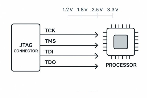
This adaptive voltage scheme is essential in modern electronics. The JTAG interface must match the specific I/O voltage rail of the processor's JTAG pins. This is accomplished through a reference voltage pin on the JTAG header, typically labeled VREF or VTARG. The debugger senses this voltage and automatically adjusts its internal drivers and receivers to match. I learned this the hard way years ago when I connected an old 5V-only parallel port JTAG adapter to a new 2.5V FPGA. The result was a puff of smoke and a very dead chip. Modern debuggers with VREF sensing prevent these costly mistakes.
Distinguishing Between I/O Voltage (VCCIO) and Core Voltage (VCORE)
A critical point for hardware designers is connecting the JTAG VREF pin to the correct supply rail. Modern processors have at least two different voltages: a low core voltage (VCORE), often 0.9V to 1.2V, that powers the internal logic, and a higher I/O voltage (VCCIO), often 1.8V or 3.3V, that powers the pin drivers. The JTAG interface signals are part of the I/O, so VREF must be connected to the I/O voltage (VCCIO), not the core voltage. Connecting VREF to VCORE is a common design error that will lead to JTAG communication failure.
| Logic Family | Typical Voltage | Common Use Case |
|---|---|---|
| TTL | 5V | Legacy systems, older microcontrollers |
| LVCMOS | 3.3V | General-purpose MCUs, FPGAs, peripherals |
| LVCMOS | 2.5V | High-speed I/O, some FPGAs and processors |
| LVCMOS | 1.8V | Modern CPUs, FPGAs, DDR memory interfaces |
| LVCMOS | 1.2V | Advanced processor cores and high-speed interfaces |
What Is JTAG and What Is It Used For?
Feeling like you're debugging in the dark? JTAG offers a powerful window into your hardware. It's a standardized method for testing and debugging electronic circuits, giving you deep access to the inner workings of a chip.
JTAG, which stands for Joint Test Action Group (the committee that created the IEEE 1149.1 standard), is primarily used for in-circuit debugging, boundary-scan testing of printed circuit board (PCB) interconnects, and programming programmable devices like FPGAs and CPLDs.
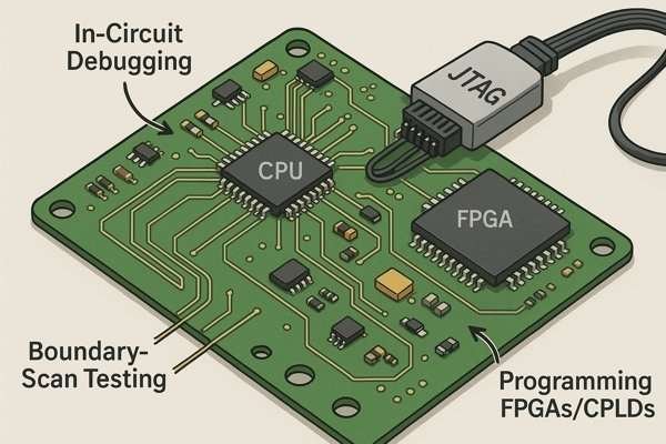
The original purpose of JTAG was not debugging, but solving a physical testing problem. As components shrank and surface-mount technology (SMT) became common, the traditional "bed-of-nails1" method of testing PCBs, which required physical contact with every pin, became impossible. JTAG, or boundary-scan, was invented to solve this. It places a small test cell right at each I/O pin inside the chip. These cells can be linked together to form a virtual "wire" that snakes around the perimeter of the chip, allowing signals to be controlled and observed without physical probes. It was such a powerful access method that engineers quickly realized this "test port" could also be used to halt the processor, inspect its internal state, and control its execution—and thus, the modern JTAG debug port was born.
The Problem JTAG Solved: In-Circuit Testing on Dense PCBs
Before JTAG, testing a populated PCB meant pressing it down onto a fixture with hundreds of spring-loaded "pogo" pins. This became impractical with the rise of Ball Grid Array (BGA) packages, where the connections are hidden underneath the chip. Boundary-scan allows for comprehensive testing of these connections. By instructing a pin on one chip to drive high and then reading the state of the corresponding pin on another chip through the scan chain, you can verify the connection between them is intact.
From a Testing Protocol to a Debugging and Programming Tool
The Test Access Port (TAP) provided a gateway into the chip. The hardware and firmware community adapted this test functionality to create powerful in-circuit emulators and debuggers. Instead of just controlling I/O pins, special JTAG instructions were created to access the processor core itself. This enabled the features we rely on today, such as setting breakpoints, single-stepping through code, and viewing memory.
| Application | Description |
|---|---|
| Boundary-Scan Testing | Verifies PCB solder joints and traces between JTAG-compliant devices. |
| In-Circuit Debugging | Halts the CPU, steps through code, inspects registers and memory. |
| Device Programming | Programs firmware into flash memory or configuration data into FPGAs/CPLDs. |
What Are the Standard JTAG Pin Names?
Ever been confused by the alphabet soup of JTAG pin labels on a schematic? Knowing the role of each pin is the first step to a successful connection. Each has a distinct and vital function in the JTAG communication protocol.
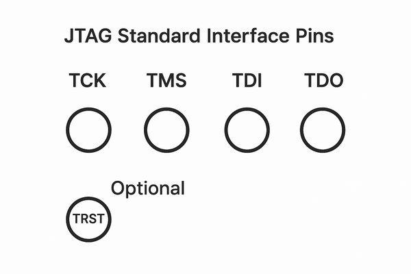
The standard JTAG interface consists of four mandatory pins: TCK (Test Clock), TMS (Test Mode Select), TDI (Test Data In), and TDO (Test Data Out). An optional fifth pin, TRST (Test Reset), is also common.
These pins form the Test Access Port (TAP) and are the physical interface to the JTAG state machine inside the target device. I once spent a frustrating afternoon trying to debug a board, only to discover that I had swapped the TDI and TDO connections on the schematic. It's a simple mistake, but one that completely prevents communication. Understanding the flow of information—clock and mode from the debugger, data in on TDI, and data out on TDO—is fundamental to both hardware design and the debugging process.
Functions of the Four Core JTAG Signals
The four mandatory signals are the heart of the JTAG protocol.
- TCK (Test Clock): The clock that synchronizes all JTAG operations.
- TMS (Test Mode Select): The control signal that navigates the TAP state machine.
- TDI (Test Data In): The serial data input to the target.
- TDO (Test Data Out): The serial data output from the target. An important detail is that the TDO pin is tri-stated (put into a high-impedance state) by any device that is not actively selected and shifting out data. In a multi-device chain, only one device drives TDO at a time. This is why an external pull-up resistor on the TDO line is crucial to maintain a valid logic level when it's not being driven.
The Role of Optional and System-Level Reset Pins
While not required, reset pins are common and useful.
- TRST (Test Reset): An active-low pin providing an asynchronous hardware reset of the TAP controller. It's optional because the same reset state can be reached by holding TMS high for 5 TCK cycles.
- SRST (System Reset): Often included on JTAG headers but not part of the JTAG standard. It allows the debugger to reset the entire processor, which is extremely useful for restarting the target in a known state.
How Is a JTAG Debugger Connected to a Target Device?
Got your JTAG debugger, but not sure how to hook it up? The physical connection is just as important as the electrical one. Using the correct connector and cable is crucial for a stable and reliable debugging session.
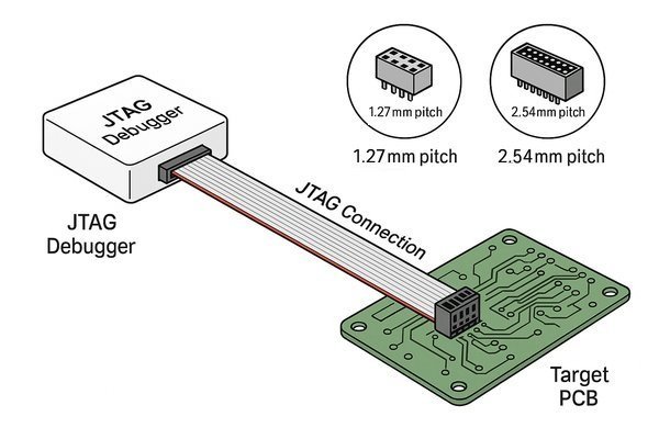
A JTAG debugger is connected to the target device via a ribbon cable that plugs into a JTAG header on the PCB. These headers come in various pin counts and pitches, with common configurations being 10-pin (2x5) and 20-pin (2x10) with 1.27mm or 2.54mm spacing.
A frustrating reality of JTAG is that while the electrical signals are standardized, the physical connector is not. This has led to a variety of "de facto" standards. When designing a new PCB, I always try to use the most common connector for my target architecture. It's also critical to place the header in an accessible location. I once designed a board where the JTAG header was perfectly placed, only to find it was completely blocked when the board was installed in its metal enclosure, forcing a painful last-minute redesign.
Using Keyed Connectors to Prevent Connection Errors
To prevent plugging in the ribbon cable backward, which can damage the hardware, most modern JTAG headers are shrouded and keyed. The plastic shroud around the pins has a notch, and the corresponding cable connector has a bump that fits into the notch. This physical polarization ensures the cable can only be connected in the correct orientation. I strongly recommend using keyed headers in all your designs.
A Look at Common JTAG Connector Pinouts
The pinout is what truly matters. Always check the documentation for your debugger and your target device.
| Pin # | ARM 10-Pin (1.27mm) | ARM 20-Pin (2.54mm) | TI 14-Pin (2.54mm) |
|---|---|---|---|
| 1 | VTARG (VREF) | VTARG (VREF) | TMS |
| 2 | GND | GND | TDI |
| 3 | TMS / SWDIO | TRST | TDO |
| 4 | GND | GND | TCK |
| 5 | TCK / SWCLK | TDO | GND |
| 7 | TDO / SWO | RTCK | EMU0 |
| 11 | - | SRST | TRST |
| 13 | - | TDI | VTARG (VREF) |
Do JTAG Signals Require Pull-Up or Pull-Down Resistors?
Wondering if you need to add extra components to your JTAG lines? A floating JTAG pin can cause unpredictable behavior, leading to system crashes and frustrating debugging sessions that go nowhere.
Yes, it is highly recommended to use pull-up and pull-down resistors on the JTAG signal lines. A pull-up resistor (typically 4.7kΩ to 10kΩ) should be used on TMS, TDI, TDO, and the optional TRST. A pull-down resistor (also 4.7kΩ to 10kΩ) is recommended for TCK.
These resistors are not merely suggestions; they are crucial for ensuring the robustness of your hardware design. They guarantee that the JTAG interface is in a known, safe state, especially when no debugger is connected. Omitting them is a common mistake that can lead to intermittent, hard-to-diagnose failures. On one project early in my career, a missing pull-down on TCK caused random boot failures that we chased for days. It turned out that environmental noise on the floating clock line was occasionally interpreted as a valid clock signal, pushing the JTAG state machine into an unknown state and halting the processor. This experience taught me that these few cents worth of resistors are some of the best insurance an engineer can buy.
Why Pull Resistors Are Essential for the JTAG TAP Controller
The core of the JTAG interface is the Test Access Port (TAP) controller, which is a state machine defined by the IEEE 1149.1 standard. The transitions between states are controlled by the TMS signal on the rising edge of TCK. A pull-up on TMS is critical because when a debugger is disconnected, the pin is held high. According to the state diagram, holding TMS high for five or more TCK cycles will always force the TAP controller into the Test-Logic-Reset state. This is the safest state, as it ensures the chip's core logic operates normally and is not in a debug or test mode. Without a pull-up, a floating TMS pin could drift and, combined with noise on the TCK line, might cause the state machine to wander into a state that interferes with normal operation.
Selecting Pull-Up and Pull-Down Resistor Values
Choosing the right resistor values is a balance between noise immunity and power consumption. While the exact values are not highly critical, there are standard practices that ensure reliable performance.
| Signal | Recommended Pull Resistor | Typical Value Range | Rationale and Trade-offs |
|---|---|---|---|
| TMS | Pull-up to VREF | 4.7kΩ - 10kΩ | Forces TAP controller to Test-Logic-Reset state when idle. |
| TDI | Pull-up to VREF | 4.7kΩ - 10kΩ | Defines a known logic high input when no data is being driven. |
| TDO | Pull-up to VREF | 4.7kΩ - 10kΩ | Prevents the line from floating as TDO is tri-stated by devices not being addressed. |
| TCK | Pull-down to GND | 4.7kΩ - 10kΩ | Prevents false clocking from noise/crosstalk. A stable low state is crucial. |
| TRST (Optional) | Pull-up to VREF | 4.7kΩ - 10kΩ | TRST is active-low. A pull-up de-asserts the reset, ensuring the TAP is operational. |
How Does a JTAG Debugger Detect the Target's Voltage?
Ever plugged in a JTAG debugger and had it just work, without you setting any voltage? This isn't magic. The debugger has a clever way of automatically adapting to your target's specific power requirements to prevent any damage.
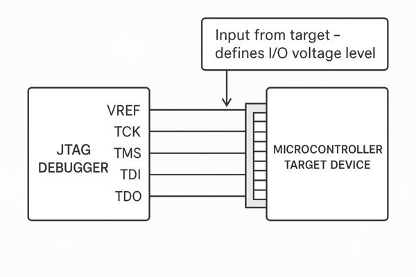
A JTAG debugger detects the target's I/O voltage through a dedicated reference voltage pin on the JTAG connector, commonly labeled as VREF, VTARG, or VTRef. This pin is connected to the I/O voltage rail of the target device.
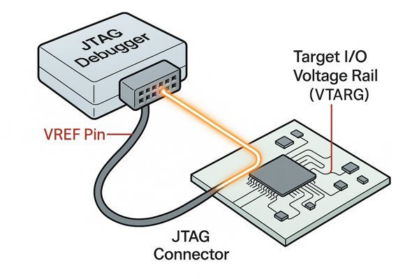
This VREF pin is the key to modern, multi-voltage debugging. It is a critical input to the debugger. The debugger doesn't supply power through this pin; it only senses the voltage level that the target board provides. This single measurement allows the debugger to configure its internal hardware to match the target's logic levels perfectly. I always make it a point during board bring-up to probe the VREF pin on the JTAG header with a multimeter before connecting my expensive debugger for the first time. It's a simple sanity check that ensures the power rail is correct and can save you from a very bad day.
The Role of Internal Debugger Level Shifters
Modern debuggers contain integrated circuits called level shifters2 or voltage translators. These chips have separate power rails for their input and output sides. The VREF signal from the target board is used to power the output side of these shifters. This ensures that any signal the debugger sends to the target (TCK, TMS, TDI) will have a logic high equal to the target's VREF. Similarly, it sets the voltage threshold for interpreting the logic levels of signals coming from the target (TDO).
Consequences of an Incorrect VREF Connection
A misconfigured VREF is a common source of JTAG failures.
| VREF Condition | Symptom | Reason / Consequence |
|---|---|---|
| Not Connected (0V) | Debugger reports "Target not powered" or "Cannot connect". | The debugger sees 0V and assumes the board is off, refusing to start a session. |
| Connected to Wrong Rail (Too High) | Target device may be permanently damaged. | Driving 3.3V signals into a 1.8V chip can destroy the input protection diodes and damage the chip. |
| Connected to Wrong Rail (Too Low) | Unreliable communication or connection failure. | Driving 1.8V signals into a 3.3V chip may not be high enough to register as a valid logic '1'. |
What Is the Purpose of the VREF / VTARG Pin on a JTAG Debugger?
That VREF pin on your JTAG connector might seem minor, but it's the key to safe and reliable debugging. It's the handshake that ensures the debugger and your target board are speaking the same electrical language.
The primary purpose of the VREF (or VTARG) pin is to inform the JTAG debugger about the I/O voltage of the target device. It is an input to the debugger and is used to power the debugger's output buffers and set the threshold for its input receivers.
This pin serves two critical functions that make modern JTAG debugging both safe and versatile. In my experience, when a previously working JTAG setup suddenly fails, the first thing I check after the power supply is the VREF connection. A loose wire or a faulty connection on this one pin is often the root cause.
Ensuring Signal Compatibility Through Voltage Matching
The most important function of VREF is to enable automatic voltage matching, which is a critical safety feature. It allows the debugger to adjust its signal drivers to match the target's logic levels, preventing accidental damage. Without it, engineers would have to manually set the debugger's output voltage. It would only be a matter of time before someone forgot to change the setting from 3.3V to 1.8V when switching projects, potentially destroying the target hardware instantly. VREF makes the entire process automatic and far less error-prone.
Verifying Target Power and Connection Sequence
Before attempting to communicate, the debugger first checks for a valid voltage on the VREF pin. If it detects 0V, it will typically report an error stating that the target is not powered. This also implies a power sequence dependency: the target's I/O voltage rail must be powered up and stable before the debugger attempts to initialize the JTAG chain. Your design should ensure VREF is valid at the point of connection. This simple check prevents the debugger from attempting to drive signals into an unpowered chip, which could cause issues with latch-up or other undefined behavior.
How Is a JTAG Level Shifter Used for Mixed-Voltage Systems?
Working with a complex board that has chips running at different voltages? A JTAG level shifter is the component that bridges these electrical divides. It ensures that your JTAG signals can travel across different voltage domains without causing issues.
A JTAG level shifter, or voltage translator, is used to adapt the JTAG signal voltages when the debugger and the target device, or different devices in a JTAG chain, operate at different I/O voltage levels. It ensures that the logic high and low levels are correctly interpreted by each component.
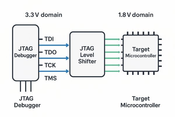
While most modern debuggers have internal level shifters, a more complex scenario arises when you have multiple devices in a JTAG daisy chain that operate at different voltages. For example, imagine a 3.3V FPGA and a 1.8V processor on the same board, connected in a single JTAG chain. The TDO signal coming out of the 3.3V FPGA cannot be safely connected to the TDI input of the 1.8V processor. This is a case where an on-board level shifter IC is required.
Designing On-Board Shifting for JTAG Daisy Chains
In a mixed-voltage daisy chain, you must place a level shifter IC between the devices. For the unidirectional signals like TCK and TMS, a simple one-way buffer is sufficient. For the TDI/TDO path, a bidirectional translator is needed. For example, the TDO of the 3.3V device connects to the high-voltage 'A' side of the shifter. The low-voltage 'B' side of the shifter then connects to the TDI of the 1.8V device. The signal path is then reversed for the return trip.
Key Features for Selecting a JTAG Level Shifter IC
When you need to implement on-board level shifting, you need a dedicated voltage translator IC.
| Feature | Importance | Why it Matters | Example Part Series |
|---|---|---|---|
| Direction Control | High | The TDI/TDO path is bidirectional in nature. Auto-direction sensing shifters simplify design. | TI TXS, NXP LSF |
| Voltage Range | High | The IC must support the specific high-side (e.g., 3.3V) and low-side (e.g., 1.8V) voltages in your design. | TI LSF, Onsemi NLSX |
| Speed (Propagation Delay) | Medium | The delay added by the shifter can limit the maximum TCK speed. For high-speed JTAG, a low-delay part is needed. | TI TXB, ADG330x |
What Is the Maximum Clock Speed (TCK) for JTAG?
Trying to speed up your JTAG programming or debugging? The TCK clock speed is a key parameter, but pushing it too high can lead to errors. Understanding the limits is essential for balancing speed and reliability.
There is no single maximum TCK speed; it is limited by the slowest device in the JTAG chain, the capabilities of the JTAG debugger, and the signal integrity of the PCB layout. Typical TCK frequencies range from 10 MHz to 100 MHz.
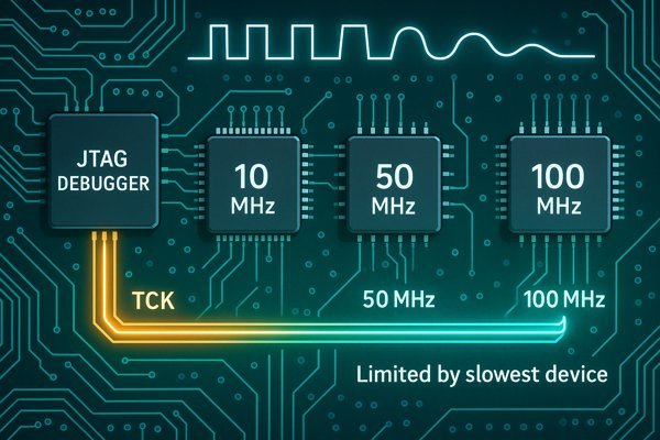
The quest for speed is common, especially when programming large flash memories. While it's tempting to crank the TCK frequency to the maximum, this often leads to a loss of reliability. I always start with a very slow, safe clock speed (like 100 kHz) to verify the connection. Then, I incrementally increase the speed until operations start failing, and finally, I back it off by 20-30% to ensure a reliable margin. The maximum stable speed is often a direct reflection of the quality of the PCB layout.
Limiting Factors and the Role of Adaptive Clocking (RTCK)
The maximum speed is dictated by the weakest link in the chain.
- Target Device: The device datasheet specifies a maximum TCK frequency.
- Debugger & Cable: The debugger's drivers and the ribbon cable itself have physical limitations.
- PCB Signal Integrity: Long traces, high capacitance, and noise are the most common culprits for limiting speed.
- RTCK (Return Test Clock): To combat these issues, some systems implement RTCK. The target receives TCK from the debugger and, after accounting for its internal delays and board delays, sends a synchronized clock signal back to the debugger on the RTCK pin. This allows the debugger to use adaptive clocking, automatically adjusting its TCK speed to the maximum that the entire system can reliably handle.
| Signal Integrity Factor | Impact on TCK Speed | Best Practice |
|---|---|---|
| Trace Length | Longer traces increase delay and degradation. | Keep JTAG traces as short as possible (< 15 cm). |
| Capacitive Loading | High capacitance rounds off clock edges. | Buffer TCK for chains with more than 4-5 devices. |
| Noise / Crosstalk | Nearby high-speed signals can corrupt JTAG signals. | Route JTAG traces away from noisy signals. |
How Are Common JTAG Connection Problems Troubleshot?
Facing a "failed to connect to target" error? JTAG connection issues can be frustrating, but a systematic approach can help you pinpoint the problem quickly. Most issues boil down to a few common culprits.
Common JTAG connection problems are often related to incorrect voltage levels (VREF), faulty physical connections, incorrect software configuration, the target being held in reset, or signal integrity issues.
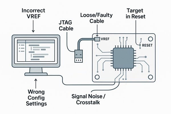
My troubleshooting process is always the same: start with the simplest things first. More than half the time, the problem is something simple like a backward cable or the board not being powered on. It's easy to assume a complex software bug when the real issue is a simple hardware oversight. Following a checklist prevents you from wasting hours chasing the wrong problem.
Troubleshooting Physical and Power Supply Issues
- Target Power & VREF: Is the board's power LED on? Use a multimeter to confirm the main voltage rails and the VREF pin are correct.
- Cable and Connector: Is the cable plugged in correctly (check Pin 1)? Is the header soldered correctly?
- Reset Lines: Is the target processor being held in a reset state by another component? Check the SRST and TRST lines.
Checking Software Settings and Target Device State
- Debugger and Target: In your IDE, have you selected the correct debugger and the specific target processor?
- TCK Speed: Set the JTAG clock speed to its lowest possible setting (e.g., 100 kHz).
- Low-Power States: A very common issue is the processor immediately entering a deep sleep or low-power mode upon boot. These modes often disable the debug clock, making JTAG connection impossible. Try connecting to the target while it is held in reset, and then release the reset.
Analyzing JTAG Signals with an Oscilloscope
If the basics check out, it's time to look at the signals.
| Symptom on Oscilloscope | Likely Cause |
|---|---|
| No clock on TCK | Faulty debugger, broken cable, or target is shorting the line. |
| TCK, TMS, TDI are active, but no signal on TDO | Wrong device in chain, device held in reset, broken TDO trace, or faulty device. |
| Signals look rounded, not sharp | Poor signal integrity (long traces, high capacitance). Try a lower TCK speed. |
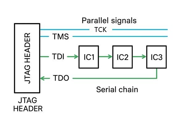
What Is a JTAG Daisy Chain?
Need to connect to multiple JTAG-compatible devices on a single board? A daisy chain is an elegant solution that saves on connector space and debugger channels. It links multiple devices into a single, scannable chain.
A JTAG daisy chain is a configuration where multiple devices are connected in series to a single JTAG header. The TCK and TMS signals are connected to all devices in parallel, while the TDI and TDO signals form a serial path through the devices.
This configuration creates one long shift register composed of all the devices on the chain. I've used this on complex telecom boards that had a main processor, an FPGA, and several CPLDs, all accessible through one JTAG port. It's an efficient way to provide test and debug access to an entire system. However, it requires careful software configuration and presents a single point of failure—if one device in the chain fails or is unpowered, the entire chain can become inaccessible.
Understanding the JTAG Daisy Chain Signal Path
- Parallel Signals (TCK, TMS): The clock and mode select signals act like a broadcast, delivered to every device simultaneously. This ensures all devices step through the TAP state machine in unison.
- Serial Path (TDI/TDO): The data path is serial. The debugger's TDI feeds the first device. The first device's TDO feeds the second device's TDI, and so on. The final device's TDO is what returns to the debugger.
How the Debugger Addresses a Specific Device in the Chain
To communicate with a single device in the chain, the debugger uses a special JTAG instruction called BYPASS. If the goal is to talk to the third device, the debugger will shift the BYPASS instruction into the Instruction Registers of the first and second devices. When a device is in BYPASS mode, its TDI and TDO pins are internally connected through a simple 1-bit register. This effectively makes the first two devices transparent (with a 1-bit delay each), allowing data to pass through them and reach the third device.
| Advantages | Disadvantages |
|---|---|
| Saves PCB space (one header for all devices). | Slower scan rates (total chain length is the sum of all devices). |
| Reduces debugger cost/complexity (one JTAG port needed). | A single fault can break the entire chain. |
| Allows for system-level interconnect testing. | Requires more complex debugger software configuration. |
| Mixed-voltage chains require on-board level shifters. |
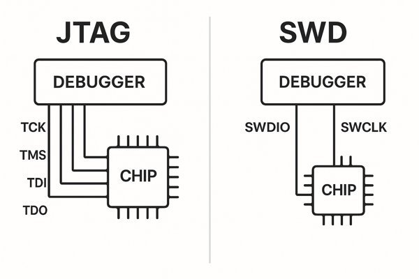
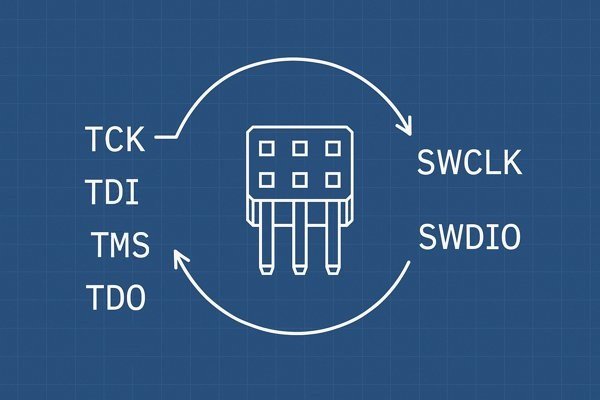
What Is the Difference Between JTAG and SWD (Serial Wire Debug)?
Working with ARM Cortex-M microcontrollers? You've likely encountered both JTAG and SWD. While they serve a similar purpose, SWD offers a more streamlined interface specifically for ARM processors.
SWD (Serial Wire Debug) is an alternative to JTAG developed by ARM. The main difference is that SWD uses only two pins (SWDIO and SWCLK) for communication, whereas JTAG requires four (TCK, TMS, TDI, TDO).
SWD was created specifically to address the need for low pin-count debugging on small, pin-constrained microcontrollers. It has become the de facto standard for the ARM Cortex-M series. While it lacks the full boundary-scan testing capabilities of JTAG, its debugging performance is on par or even faster for many operations due to its more efficient, packet-based protocol. On my own projects, I default to using SWD for ARM Cortex-M targets because it frees up I/O pins for other functions.
Comparing JTAG and SWD Protocols and Pin Count
The primary difference lies in how data is transported. JTAG is a state-machine-driven shift-register protocol using 4-5 pins. SWD, on the other hand, is a more modern, packet-based protocol that can operate with only 2 pins because its SWDIO line is bidirectional.
Real-Time Tracing with SWD's SWO Pin
Furthermore, SWD includes an optional but highly useful third signal:
- SWO (Serial Wire Output): This is a single-wire output from the target that allows the microcontroller to stream real-time trace information and
printf-style debug messages to the debugger with minimal impact on the processor's performance. This allows you to monitor variables or program flow without halting the core.
| Feature | JTAG (IEEE 1149.1) | SWD (Serial Wire Debug) |
|---|---|---|
| Pin Count | 4-5 pins | 2-3 pins |
| Boundary Scan | Yes, core feature | No, not supported |
| Real-Time Trace | No (requires separate ETM port) | Yes, via optional SWO pin |
| Target ICs | Wide support (ARM, RISC-V, FPGAs) | ARM Cortex processors only |
Want the flexibility to use either JTAG or SWD without needing separate connectors? The good news is that this is not only possible but also a common practice in modern hardware design.
Yes, JTAG and SWD can share the same connector because the SWD signals (SWCLK and SWDIO) are typically overlaid on the JTAG pins (TCK and TMS, respectively). This allows a single header, like the ARM 10-pin or 20-pin standard, to support both protocols.
This intelligent design is part of the ARM Debug Interface (ADI) standard. When laying out a PCB for an ARM processor, I can use a single standard connector (like the 10-pin Cortex Debug header) and know that it will support both protocols. This gives me the best of both worlds: I can use the efficient 2-wire SWD for everyday code development, but I can also switch my debugger to JTAG mode to perform boundary-scan tests on the production line, all through the same physical header.
How Automatic Protocol Detection Works
The sharing is made possible by a specific initialization sequence. When a debugger connects, it sends a special sequence over the SWDIO/TMS line. The debug port on the ARM chip listens for this sequence. If it detects the JTAG-to-SWD sequence, it switches to SWD mode. Otherwise, it remains in the default JTAG mode. This handshake is automatic and transparent to the user.
Pin Mapping on the Standard 10-pin Cortex Connector
The overlay is clearly defined on the standard ARM connectors.
| Pin # | Name | JTAG Function | SWD Function |
|---|---|---|---|
| 1 | VTARG/VREF | Voltage Reference | Voltage Reference |
| 3 | TMS | Test Mode Select | SWDIO (Data I/O) |
| 5 | TCK | Test Clock | SWCLK (Clock) |
| 7 | TDO | Test Data Out | SWO (Trace Output) |
| 9 | TDI | Test Data In | - (Reserved) |
Conclusion
In short, JTAG voltage is not fixed; it adapts to your target's I/O level, typically from 1.2V to 3.3V, via the VREF pin. Understanding this, along with the key pins, proper connections, and protocol differences, is fundamental to successful hardware development and debugging.


