 Skip to content
Are your power electronics designs hitting their thermal and current limits? You are pushing more power through smaller boards, but standard PCBs just can't handle the load, leading to overheating and potential failure.
The primary benefit of a heavy copper PCB is its ability to carry significantly higher currents and manage heat more effectively than a standard PCB. This allows for more compact and reliable power circuits by integrating high-current traces directly into the board, reducing the need for bulky wires or bus bars.

I’ve seen many projects struggle when a standard 1-ounce or 2-ounce copper board is pushed beyond its limits. The design might work on the bench for a short time, but it's a field failure waiting to happen. Understanding when to step up to a heavy copper design is a critical skill for any hardware engineer working on power systems. It’s not just about making traces wider; it’s about fundamentally changing how the board manages current and heat. Let's dive into the specifics of what makes these boards different and when you should consider them.
What Qualifies as a Heavy Copper PCB?
Struggling to define when a PCB officially becomes "heavy copper"? The terminology can seem vague, leaving you unsure if your 3 oz design truly fits into this category or if it's just a slightly thicker standard board.
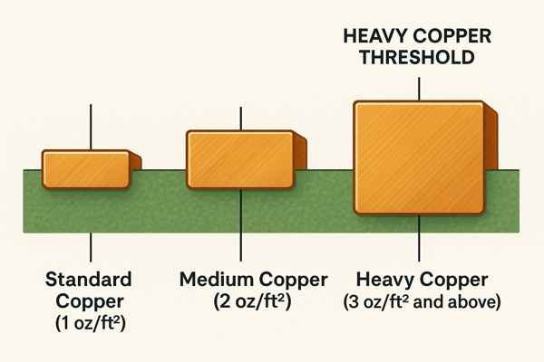
A printed circuit board is classified as a heavy copper PCB when the copper weight of its inner or outer layers is 3 ounces per square foot (oz/ft²) or more. While 2 oz copper is thicker than standard, 3 oz is the generally accepted industry starting point for the "heavy copper" classification.
Understanding Copper Weight Classifications
The term "ounce" in PCB manufacturing can be confusing at first. It's a measure of weight distributed over an area, which translates directly to thickness. One ounce of copper spread over one square foot (ft²) of laminate results in a copper layer that is 1.37 mils (or about 35 micrometers) thick.
The industry uses a few key classifications for copper weight:
| Category | Copper Weight (oz/ft²) | Typical Thickness (mils / µm) |
|---|---|---|
| Standard Copper | 0.5 oz to 2 oz | 0.69 - 2.74 mils / 17.5 - 70 µm |
| Heavy Copper | 3 oz to 19 oz | 4.11 - 26.03 mils / 105 - 483 µm |
| Extreme Copper | 20 oz to 200 oz | 27.4 - 274 mils / 696 - 6960 µm |
These definitions are generally consistent with industry practices and guidelines from bodies like the IPC (Association Connecting Electronics Industries). While a 2 oz board offers improved performance over the common 1 oz, the manufacturing processes for 3 oz and above, like differential etching and high-speed plating, are significantly different, justifying the separate "heavy copper" category.
What Is the Maximum Copper Weight for a PCB?
Are you designing a system with extreme current demands? You may wonder what the absolute physical limit is for copper thickness on a PCB, and if it's even possible to manufacture a board that meets your high-power requirements.
While theoretically very high, the practical maximum copper weight for a PCB is typically around 200 oz/ft² (approximately 6.96 mm or 0.274 inches thick). Manufacturing boards this thick requires highly specialized and expensive lamination and plating processes, making it a solution for very specific, extreme-power applications.

Scaling Up: Manufacturing Challenges
For most industrial applications, copper weights between 3 oz and 10 oz are common and provide a good balance of performance and manufacturability. As you go beyond 20 oz, you enter the realm of "Extreme Copper." Creating these boards is more like metal forming than standard PCB etching.
Here’s how the manufacturing challenges scale with copper weight:
- 3-6 oz: Achievable with most advanced PCB fabricators. Requires precise etching control to manage undercut and maintain trace definition.
- 7-19 oz: Requires specialized equipment. Lamination of multiple pre-etched copper layers is often necessary, and achieving fine features becomes very difficult.
- 20-200 oz: This is a niche capability. These boards are often made by bonding heavy copper plates to a substrate and then milling the circuit pattern, rather than etching. The end product often resembles a machined metal part more than a traditional PCB.
In my experience at Honeywell, we designed power distribution boards for security panels that used 4 oz and 5 oz copper. This was sufficient to handle high inrush currents for sirens and strobes without needing separate bus bars, saving space and assembly costs. Pushing beyond that requires a very strong justification due to the rapidly increasing cost and design constraints.
How Does Heavy Copper Affect PCB Thermal Management?
Is your main processor or power FET overheating despite a large heatsink? You might be overlooking the board itself, which can act as a thermal bottleneck, trapping heat and degrading component performance and reliability.
Heavy copper layers drastically improve thermal management by transforming the PCB into an efficient heat sink. Copper's high thermal conductivity (around 400 W/m·K) allows it to pull heat away from hot components and spread it across a larger area of the board, significantly lowering component operating temperatures.

The Physics of Heat Spreading
The difference in thermal performance is staggering when you compare copper to the standard FR-4 substrate. FR-4 has a thermal conductivity1 of only about 0.25 W/m·K, making it a very effective insulator. This is over 1000 times less conductive than copper.
In a standard 1 oz PCB, the thin copper layer has a limited ability to conduct heat laterally. When you use a 4 oz or 6 oz copper plane, you create a thick, highly conductive thermal path. This path can be just as effective, and sometimes more so, than a traditional aluminum heat sink.
Consider this example:
A power MOSFET is mounted on a PCB.
- On a 1 oz Board: Heat from the MOSFET creates a small, intense hotspot directly under the component. The FR-4 below does little to help, and the thin copper traces can't pull the heat away fast enough. The component's temperature might rise by 50°C above ambient.
- On a 4 oz Board: The heavy copper ground plane connected to the MOSFET's thermal pad acts like a heat spreader2. Heat is rapidly pulled away from the component and distributed across the entire plane. The temperature rise might be reduced to just 20°C above ambient.
This effect allows you to potentially eliminate external heat sinks, reduce fan requirements, and build more compact and robust products. We used this principle extensively in designing fanless industrial controllers.
What Is the Current-Carrying Capacity of Heavy Copper Traces?
Have your standard PCB traces burned out under high load? Calculating the right trace width is critical, but the old rules of thumb often fall short, especially when dealing with the higher currents that heavy copper allows.
The current-carrying capacity of a heavy copper trace is determined by its cross-sectional area and the acceptable temperature rise. According to the IPC-2152 standard, a 4 oz copper trace can carry roughly 2-3 times more current than a 1 oz copper trace of the same width for the same temperature rise.

Current Capacity by the Numbers
IPC-21523 is the modern standard for determining the relationship between current, trace temperature, and conductor size. It's far more comprehensive than the older IPC-2221 standard because it accounts for the influence of the board material and nearby copper planes.
Let's look at a practical comparison based on the IPC-2152 guidelines for an external trace with a 20°C temperature rise over ambient:
| Trace Width | Current Capacity (1 oz Copper) | Current Capacity (4 oz Copper) |
|---|---|---|
| 50 mil (1.27 mm) | ~3.5 Amps | ~8.0 Amps |
| 100 mil (2.54 mm) | ~5.5 Amps | ~13.0 Amps |
| 200 mil (5.08 mm) | ~8.5 Amps | ~21.0 Amps |
| 500 mil (12.7 mm) | ~15.0 Amps | ~38.0 Amps |
Note: These are approximate values. The exact capacity depends on board thickness, proximity to other copper features, and whether the trace is on an internal or external layer.
As you can see, quadrupling the copper thickness (from 1 oz to 4 oz) does not quadruple the current capacity. This is because as the trace gets thicker, its surface area for convection cooling doesn't increase proportionally. However, the increase is still substantial. Using heavy copper allows you to design for high currents without needing excessively wide traces, which is crucial for keeping board size down.
What Are the Common Applications for Heavy Copper PCBs?
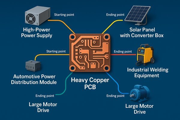
Wondering where these robust boards are actually used? You might be surprised to find that heavy copper PCBs are the backbone of many high-power systems that you encounter daily, often hidden away from view.
Heavy copper PCBs are most commonly used in high-power and high-current applications where thermal performance and reliability are critical. Key examples include power supplies, solar power converters, automotive power distribution centers, welding equipment, and industrial motor drives.
Key Application Areas
The unique ability of heavy copper to manage both high currents and the resulting heat makes it essential in a wide range of fields. I’ve seen them deployed in some of the most demanding environments.
| Industry Vertical | Specific Applications | Why Heavy Copper is Used |
|---|---|---|
| Power Electronics | SMPS, UPS, Planar Transformers | High current density, thermal spreading, integrated windings. |
| Industrial Automation | Motor Drives, Welding Controls, PLCs | Durability, high current handling, heat dissipation in harsh environments. |
| Automotive & Aerospace | EV Battery Systems, Power Distribution | Reliability under vibration and thermal stress, space savings. |
| Renewable Energy | Solar Inverters, Wind Turbine Converters | Efficiency, managing high currents from panels, thermal stability. |
| Medical Devices | MRI/CT Scanners, Surgical Tools | Reliability, low noise (via large ground planes), thermal management. |
In essence, if a design needs to move a lot of current (typically >10A) reliably and stay cool without a massive cooling system, a heavy copper PCB is often the best solution.
Are There Specific Design Rules for Heavy Copper Circuit Boards?
Are you assuming you can design a 4 oz board the same way you design a 1 oz board? This is a common mistake. Heavy copper introduces new manufacturing constraints that require specific design rules for spacing, trace width, and clearances.
Yes, there are critical design rules specific to heavy copper boards. You must account for larger trace-to-trace and trace-to-pad clearances to prevent shorting, use thermal reliefs on through-hole pads to enable soldering, and respect the manufacturer's minimum feature size, which is larger than on standard PCBs due to etching challenges.

Critical Design Rules for Manufacturability
When you etch thick copper, more etchant is required, and it tends to remove some copper from the sides of the trace as it etches downwards. This is called "undercut." To compensate, manufacturers start with a wider trace on the artwork than the desired final width. This entire process limits how close features can be to each other.
Here are key design rules to follow:
| Design Rule | Standard PCB (1 oz) | Heavy Copper PCB (4 oz) | Reason for Change |
|---|---|---|---|
| Minimum Trace/Space | 3/3 mil (0.076mm) | 8/8 mil (0.203mm) or more | To compensate for etching undercut and prevent shorts. |
| Annular Ring (Min) | 1 mil (0.025mm) | 8 mil (0.203mm) | Ensures a solid connection after drilling through thick copper. |
| Pad to Copper Clearance | 8 mil (0.203mm) | 15-20 mil (0.38-0.51mm) | Prevents shorts and provides isolation for high-voltage planes. |
| Thermal Reliefs | Optional / 10 mil spokes | Essential / 20 mil spokes | Thick copper planes act as massive heat sinks, making soldering impossible without thermal reliefs4 that limit heat flow away from the pad. |
I once had a junior engineer send a 4 oz design to a fab without proper thermal reliefs on the connector pads. The assembly house called us, completely unable to solder the parts. The board's ground plane was sinking all the heat from their soldering irons. We had to scrap the entire batch of bare boards and redesign them correctly. It was an expensive lesson in remembering that heavy copper changes everything, right down to basic assembly.
What Are the Challenges of Soldering Heavy Copper Boards?
Having trouble getting a good solder joint on your heavy copper prototype? If your soldering iron feels like it's doing nothing, you're experiencing the primary challenge: the board's massive thermal conductivity is fighting you every step of the way.
The main challenge of soldering heavy copper boards is their extremely high thermal mass. The thick copper planes act as powerful heat sinks, drawing heat away from the soldering iron tip so quickly that it's difficult to get the pad and component lead up to the reflow temperature of the solder.

Soldering Strategies for High Thermal Mass
The heat-sinking effect can lead to several common assembly defects. To successfully solder heavy copper boards, you need to anticipate these issues and adjust your process accordingly.
| Challenge | Consequence | Solution |
|---|---|---|
| Massive Heat Sinking | Inability to reach solder reflow temperature. | Preheat the board to 120-150°C. Use a high-power (100W+) soldering station. |
| Cold Solder Joints5 | Weak, brittle, unreliable electrical connection. | Use a larger soldering tip for better heat transfer and apply active flux. |
| Extended Dwell Time | Risk of damaging components or the PCB laminate. | Preheating is key. It minimizes the time the iron needs to be on the joint. |
| Component Tombstoning6 | Component lifts off one pad during reflow. | Ensure proper thermal relief design on pads connected to large planes. |
For production, a carefully profiled reflow oven is essential. The temperature profile must include a proper preheat/soak stage to ensure the entire board reaches a uniform temperature before hitting the final reflow peak.
Heavy Copper PCB vs. Standard PCB: What Are the Key Differences?
Trying to decide between a standard board and a heavy copper one? While they may look similar at a glance, their capabilities, costs, and applications are worlds apart, and choosing the wrong one can doom your project.
The key difference lies in the copper thickness, which dictates current capacity, thermal performance, and cost. A heavy copper PCB uses 3 oz or more of copper, enabling high-current circuits and effective heat dissipation, while a standard PCB uses 2 oz or less, suiting low-power digital and analog applications.

A Head-to-Head Comparison
Choosing between them requires a clear understanding of the trade-offs. I’ve summarized the most important differences in this table to help you make an informed decision for your next project.
| Feature | Standard PCB | Heavy Copper PCB |
|---|---|---|
| Copper Weight | 0.5 oz - 2 oz | 3 oz - 200 oz |
| Max Current | Low to Medium (Typically < 10A per trace) | High to Extreme (Can exceed 100A) |
| Thermal Management | Poor. FR-4 is an insulator. Relies on vias and small planes. | Excellent. Copper planes act as built-in heat sinks. |
| Fabrication | Standard etching process, fine features possible (3/3 mil). | Specialized differential etching, requires wider trace/space (e.g., 8/8 mil). |
| Cost | Low. Standardized, high-volume process. | High. More raw material and complex, lower-yield processes. |
| Common Applications | Microcontrollers, logic circuits, sensors, RF. | Power supplies, motor drives, inverters, power distribution. |
| Soldering | Easy. Low thermal mass. | Challenging. High thermal mass requires preheating and powerful tools. |
In my work on medical infusion pumps, we used a standard 4-layer, 1 oz PCB for the control and display logic. But for the motor drive and battery charging circuit, we used a separate 2-layer, 4 oz heavy copper board. This "hybrid" approach allowed us to optimize cost and performance, using the right technology for each specific function. It's not always an all-or-nothing choice.
What Is the Cost of Heavy Copper PCBs Compared to Standard Ones?
Worried about the budget for your next power project? You know heavy copper is more expensive, but "more" isn't a useful number. You need a realistic cost estimate to determine if the benefits justify the expense.
A heavy copper PCB is significantly more expensive than a standard board, but the cost doesn't scale linearly. For small prototype quantities, a 4 oz heavy copper board might cost 4 to 6 times more than an equivalent 1 oz standard board due to process complexity and material cost.

A Practical Cost Breakdown
Let's break this down with a concrete example for a small prototype run of 5 boards, with a size of 100mm x 100mm (2 layers):
-
Standard 1 oz Copper PCB:
- Base Material Cost: Low
- Processing: Standard, high-yield automated process.
- Estimated Prototype Cost: $25 - $50
-
Heavy 4 oz Copper PCB:
- Base Material Cost: Higher (4x the copper).
- Processing: Requires special etching and plating steps, more manual inspection, and lower panel yield.
- Estimated Prototype Cost: $120 - $200
As you can see, the jump is substantial. The primary cost drivers for heavy copper are not just the raw material, but the specialized manufacturing processes. These processes are slower, require more skilled labor, and have a lower yield, meaning more boards on a production panel might fail inspection.
However, it's crucial to evaluate the system-level cost. If using a $150 heavy copper board allows you to eliminate a $20 heatsink, a $5 fan, a $10 bus bar, and the associated assembly labor and connectors, the more expensive PCB might actually be the more cost-effective solution. You are integrating mechanical components directly into the PCB, simplifying the BOM and assembly.
What Are the Alternatives to Heavy Copper for High-Current Applications?
Is a heavy copper PCB too expensive or not quite right for your design? Before you commit, it's important to know the alternatives. There are other ways to manage high currents, each with its own set of advantages and disadvantages.
The main alternatives to heavy copper PCBs for high-current applications are external bus bars, high-current wires and cables, and specialized embedded copper components. The best choice depends on the specific current level, mechanical requirements, and cost targets of your project.

Exploring High-Current Alternatives
Let's explore the most common alternatives and when to use them. I've often had to choose between these options based on the project's unique constraints.
| Alternative | Description | Best For... | Pros | Cons |
|---|---|---|---|---|
| Bus Bars | Solid or laminated metal bars (usually copper or aluminum) that are bolted or soldered to the PCB. | Extremely high currents (>100A), applications requiring field serviceability or mechanical rigidity. | Highest current capacity, excellent heat dissipation, very robust. | Bulky, adds assembly steps and cost, requires manual installation. |
| Wires/Cables | Point-to-point wiring using thick-gauge cables that are soldered or crimped to the board. | Connecting separate modules, applications where flexibility is needed, or for a few high-current paths on a mostly low-power board. | Flexible, readily available, easy to implement for simple connections. | Can be messy, prone to vibration failure, manual assembly is error-prone and costly. |
| Embedded Copper | Embedding pre-formed copper coins, inlays, or bus bars into the PCB during lamination. | Very high, localized current density where a surface trace isn't enough. For example, under a power FET. | Excellent thermal transfer, integrates directly into the PCB, saves space. | Very expensive, complex manufacturing, locks you into a specific fabricator. |
In one industrial automation project, we had a central control board that needed to distribute 50A to several motor drivers. A full 6 oz heavy copper board was too costly. Instead, we used a standard 2 oz board for all the logic and mounted a custom-stamped copper bus bar directly onto the PCB with press-fit terminals. This gave us the high-current capability we needed without the cost of a fully heavy copper design.
When Should I Use Bus Bars Instead of a Heavy Copper PCB?
Are you debating between a 10 oz copper PCB and a screw-on bus bar? Making the wrong choice can lead to an over-engineered, expensive board or a system that is difficult to assemble and service.
You should use bus bars instead of a heavy copper PCB when you need to handle extremely high currents (typically over 100-200A), require a mechanically robust distribution point, or need the ability to easily connect and disconnect high-power cables in the field.

Decision Guide: Heavy Copper vs. Bus Bars
While heavy copper PCBs are powerful, they have their limits. Bus bars take over where even the thickest PCBs fall short. The decision to use one over the other comes down to three main factors: Current, Mechanical Strength, and Serviceability.
| Use a Heavy Copper PCB When... | Use Bus Bars When... |
|---|---|
| Current is generally below 100A. | Current is consistently above 100A. |
| You need to integrate power and logic on one board. | The power entry point needs to be a rigid structural element. |
| Space is tight and you want a compact solution. | You need to connect large cables with screw terminals. |
| The design is self-contained and rarely disassembled. | Field serviceability and modularity are critical. |
| Reducing BOM part count is a key goal. | You are connecting multiple, physically separate chassis. |
For example, in a large-scale data center rack, the main 48V power coming into the rack is distributed via massive copper bus bars. A heavy copper PCB would simply not be able to handle the thousands of amps required. However, within each server sled, a heavy copper PCB is used to distribute that 48V power to the local DC-DC converters. It's about using the right tool for the job at the right scale.
Conclusion
In summary, heavy copper PCBs are a powerful tool for managing high-current and high-power designs. They integrate power distribution and thermal management directly into the board, creating compact and reliable solutions for demanding applications.
-
Understanding thermal conductivity is crucial for optimizing heat management in electronic designs. Explore this link for in-depth insights. ↩
-
Learn about heat spreaders and their role in thermal management, which can help you design more efficient electronic devices. ↩
-
Explore this link to understand the IPC-2152 standard, which is essential for determining current capacity in PCB design. ↩
-
Exploring the importance of thermal reliefs can help prevent soldering issues and improve PCB performance. ↩
-
Preventing cold solder joints is crucial for reliable connections; explore effective strategies to enhance your soldering skills. ↩
-
Learn about tombstoning causes to avoid this common issue and ensure better soldering results in your projects. ↩


