 Skip to content
Struggling with environmental regulations? Choosing the right PCB surface finish is key. Many common finishes now meet RoHS standards, helping you stay compliant.
Most widely used RoHS compliant PCB surface finishes include Lead-Free HASL, ENIG (Electroless Nickel Immersion Gold), ENEPIG (Electroless Nickel Electroless Palladium Immersion Gold), Immersion Silver (ImAg), Immersion Tin (ImSn), and OSP (Organic Solderability Preservatives). These finishes avoid the restricted substances outlined in the RoHS directive.

Keeping up with environmental directives like RoHS is a big part of our job as hardware engineers. It's not just about picking a finish that works; it has to be compliant too. I remember a project early in my career where we had to scramble to find a RoHS compliant alternative for a legacy product. It taught me the importance of considering these factors from the very beginning of the design cycle. Let's explore some of these compliant finishes and other related concerns.
What Causes "Black Pad" Syndrome in ENIG, and How Can It Be Prevented?
Ever had a BGA fail unexpectedly after assembly, even when X-rays looked fine? "Black pad" syndrome in ENIG can be a frustrating, hidden defect.
"Black pad" syndrome is primarily caused by corrosion of the nickel layer beneath the gold in an ENIG finish. This often results from an overly aggressive immersion gold bath, incorrect phosphorus content in the nickel, or contaminants. It leads to a weakened, non-wettable nickel surface, causing poor solder joints.
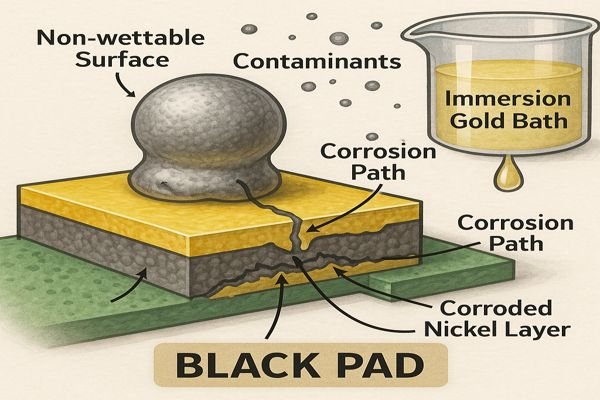
This issue can be a real headache. You think everything is perfect, the boards look good, but then you start seeing intermittent failures or components lifting off pads, especially BGAs. The "black pad" itself isn't always visible before soldering because the gold layer covers it. It's only after the gold dissolves into the solder during reflow that the compromised nickel surface is exposed, leading to a weak or failed joint.
Black Pad in ENIG: A Closer Look at Causes and Prevention
The term "black pad" refers to the dark, corroded appearance of the nickel pad surface once the overlying gold and solder are removed from a failed joint. It's a complex issue with several contributing factors rooted in the ENIG plating process.
Key Causes:
-
Phosphorus Content in Electroless Nickel (EN) Bath:
- The phosphorus content in the nickel layer is crucial. Typically, a phosphorus level of \(7-9\%\) (by weight) is considered optimal for good solderability and corrosion resistance. According to IPC-4552B, "Specification for Electroless Nickel/Immersion Gold (ENIG) Plating for Printed Boards," the typical range for phosphorus in the nickel deposit is \(6-10\%\) by weight, although some fabricators target a narrower range within this.
- If the phosphorus content is too high (e.g., \(>10-11\%\)), it can make the nickel layer more prone to corrosion during the immersion gold (IG) plating step. This is because the gold bath is an acidic, replacement reaction.
- Conversely, very low phosphorus content (\(<6\%\)) can make the nickel layer brittle and more susceptible to fracture.
- Maintaining phosphorus within a well-controlled range, often recommended by plating chemistry suppliers (e.g., \(7-9\%\) as cited in many technical papers on the subject), significantly reduces black pad occurrences.
-
Immersion Gold (IG) Bath Aggressiveness:
- The immersion gold process is a galvanic displacement reaction where nickel atoms are displaced by gold atoms. If this reaction is too aggressive (e.g., due to high gold concentration, incorrect \(\text{pH}\), or contaminants), it can excessively corrode the nickel surface.
- IPC-4552B specifies gold thickness typically between \(0.05 \mu\text{m}\) to \(0.125 \mu\text{m}\) (\(2 \text{ to } 5 \mu\text{inches}\)). If the gold deposition process is too aggressive or prolonged in an attempt to achieve thicker gold beyond specification, it can lead to hyper-corrosion of the nickel. The standard itself cautions against overly thick gold for this reason.
-
Contamination:
- Contaminants in either the EN or IG baths can disrupt the plating process and lead to localized corrosion or a compromised nickel structure.
- Poor rinsing between plating steps can also carry over chemicals that interfere with subsequent processes. For example, residual palladium activators (if used prior to EN) or EN bath constituents can negatively impact the IG step.
-
Process Control:
- Tight control over bath chemistry (\(\text{pH}\), temperature, metal concentrations, stabilizer levels) and immersion times is critical. Deviations can quickly lead to problems. For example, the nickel bath temperature is typically around \(85-90^{\circ}\text{C}\) (\(185-194^{\circ}\text{F}\)), and the gold bath around \(80-85^{\circ}\text{C}\) (\(176-185^{\circ}\text{F}\)), as per general industry practice and chemistry supplier datasheets.
Prevention Strategies:
To prevent black pad, a multi-faceted approach focusing on strict process control during PCB fabrication is necessary:
| Prevention Aspect | Key Actions | Target Values/Parameters (Examples) | Source/Standard Reference |
|---|---|---|---|
| Nickel Bath Control | Maintain optimal phosphorus content, temperature, \(\text{pH}\), and nickel concentration. Regular bath analysis and replenishment. | Phosphorus: \(7-9\% \text{ wt.}\), Temp: \(85-90^{\circ}\text{C}\), \(\text{pH: } 4.5-4.8\) (supplier dependent) | IPC-4552B, Plating chemistry suppliers |
| Gold Bath Control | Control gold concentration, \(\text{pH}\), temperature, and immersion time. Avoid overly aggressive bath formulations. | Gold thickness: \(0.05-0.125 \mu\text{m (2-5 }\mu\text{in)}\), Temp: \(80-85^{\circ}\text{C}\), \(\text{pH: } 4.0-5.0\) | IPC-4552B |
| Surface Preparation | Thorough cleaning and micro-etching of the copper surface before nickel plating to ensure good adhesion and remove contaminants. | Proper micro-etch rates (e.g., \(1-2 \mu\text{m}\) copper removal) | Fabrication best practices |
| Rinsing | Effective rinsing with deionized (DI) water between plating steps to prevent drag-out of bath chemistries. | High-quality DI water (e.g., \(>5 \text{ M}\Omega \cdot \text{cm resistivity}\)) | Fabrication best practices |
| Bath Maintenance | Monitor bath loading (MTOs) and replace baths before they are exhausted or byproducts build up excessively. | MTOs typically \(< 6-8\), depending on bath chemistry & supplier rec. | Plating chemistry suppliers |
| Process Monitoring | Implement Statistical Process Control (SPC) for critical plating parameters. Regular cross-sectioning and analysis of plated deposits. | Conformance to IPC-4552B requirements | IPC Standards |
By working closely with PCB fabricators who demonstrate robust process controls and a deep understanding of ENIG chemistry, the risk of black pad syndrome can be significantly minimized. I always make it a point to discuss these aspects with my suppliers, especially for high-reliability applications.
How Does PCB Surface Finish Impact Signal Integrity?
Designing for high-speed digital or RF applications? The choice of surface finish isn't just about solderability; it can significantly affect your signal integrity.
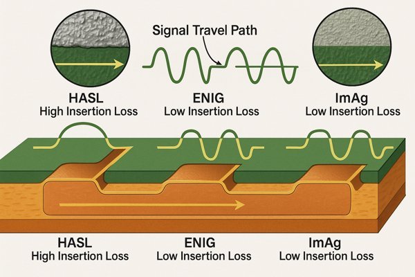
Surface finish impacts signal integrity, especially at high frequencies, primarily through the skin effect and surface roughness. Smoother finishes like ENIG or ImAg generally offer lower insertion loss compared to rougher finishes like HASL, as current concentrates on the conductor's surface.
I learned this lesson the hard way on a project involving a multi-gigabit SerDes interface. We initially used a standard finish that was fine for lower-speed signals, but we encountered unexpected signal degradation at higher data rates. After much debugging, we traced part of the problem back to the surface finish contributing to excessive insertion loss. Switching to a smoother finish made a noticeable difference.
How Surface Finishes Influence High-Speed Signals
At high frequencies, electrical current tends to flow along the outer surface or "skin" of a conductor. This phenomenon is known as the skin effect1. The depth to which the current penetrates (skin depth, \(\delta\)) decreases as frequency (\(f\)), permeability (\(\mu\)), and conductivity (\(\sigma\)) increase, described by the formula:
\(\delta = \sqrt{\frac{1}{\pi f \mu \sigma}}\)
For copper (\(\sigma \approx 5.8 \times 10^7 \text{ S/m}\), \(\mu_{r} \approx 1\)), at \(1 \text{ GHz}\), the skin depth is approximately \(2.09 \mu\text{m}\). At \(10 \text{ GHz}\), it reduces to about \(0.66 \mu\text{m}\). This means the surface characteristics of the conductor, including the plating finish, become critically important as the current is predominantly on this very thin layer.
Impact of Surface Roughness:
- Increased Conductor Losses: A rough surface effectively increases the path length for the current flowing along the surface, leading to higher resistive losses (part of insertion loss). This is often modeled using formalisms like the Morgan-Hammerstad model or Huray snowball model. For instance, a root mean square (RMS) roughness of \(1 \mu\text{m}\) can increase losses by several percent at multi-GHz frequencies compared to a perfectly smooth surface.
- Variations in Impedance: Surface roughness can also affect the local dielectric constant perceived by the signal and the physical dimensions of the trace, leading to variations in characteristic impedance. This can cause signal reflections and further degrade signal integrity.
- Increased Phase Delay: The longer effective path length on a rough surface can also introduce additional phase delay and skew between traces.
Comparing Common Finishes for High-Speed Applications:
| Surface Finish | Typical Surface Roughness (\(R_a\)) | Impact on Signal Integrity (High Frequency) | Considerations |
|---|---|---|---|
| HASL (Hot Air Solder Leveling) | High (e.g., \(1-5 \mu\text{m}\), very uneven) | Generally poor for \(> 1-2 \text{ GHz}\) due to unevenness and roughness, leading to higher insertion loss. Not recommended for controlled impedance. | Non-planar surface makes it unsuitable for fine-pitch components and high-frequency. |
| LF HASL (Lead-Free HASL) | High (e.g., \(1-5 \mu\text{m}\), very uneven) | Similar to leaded HASL; poor for high frequencies. | Same planarity issues as leaded HASL. |
| OSP (Organic Solderability Preservative) | Low (smooth copper, \(\approx 0.2-0.5 \mu\text{m } R_a\) for copper) | Good, as it's a very thin organic layer over bare copper. Copper roughness itself then becomes the dominant factor. | Limited shelf life and can be sensitive to handling. Copper surface can oxidize if OSP is compromised. |
| ImAg (Immersion Silver) | Very Low (e.g., \(<0.1 \mu\text{m } R_a\) for Ag layer) | Good to excellent. Provides a very planar and conductive surface. Silver conductivity is slightly higher than copper. Low loss. | Can tarnish if not handled or stored properly (though modern anti-tarnish agents help). Potential for electromigration under high humidity/bias. |
| ImSn (Immersion Tin) | Low to Moderate (e.g., \(\approx 0.3-0.8 \mu\text{m } R_a\)) | Fair to good. Generally smoother than HASL. | Concerns about tin whiskers, especially with pure tin finishes. Intermetallic (IMC) growth can affect long-term solderability. |
| ENIG (Electroless Nickel Immersion Gold) | Very Low (e.g., \(<0.05 \mu\text{m } R_a\) for Au layer) | Good to excellent. The gold layer is very thin and planar. The underlying nickel (\(\approx 3-6 \mu\text{m}\)) is the main current carrier at high frequencies. | Nickel is about 3-4 times more resistive than copper. The "skin effect on nickel" can lead to higher losses than a pure copper or silver surface, especially \(> 5-10 \text{ GHz}\). |
| ENEPIG (Electroless Nickel Electroless Palladium Immersion Gold) | Very Low | Very good. Similar to ENIG but palladium layer (\(0.05-0.3 \mu\text{m}\)) can offer additional benefits like better wire bondability. Palladium is also resistive. | More complex and costly than ENIG. Loss characteristics similar to ENIG due to nickel dominance. |
It's important to note that the underlying copper roughness (before any finish is applied) also plays a significant role. For very high-frequency designs (e.g., \(>10 \text{ GHz}\)), specifying low-profile (LP) or very-low-profile (VLP) copper foils can be as important, if not more so, than the choice of final finish. Standard electrodeposited (ED) copper can have an \(R_q\) (RMS roughness) of \(0.8-1.5 \mu\text{m}\) or higher on the "toothy" side, while VLP copper might be \(<0.5 \mu\text{m } R_q\). (Source: IPC and copper foil manufacturer data).
When I'm working on high-speed designs, I often prefer ENIG or ImAg for their planarity. However, for applications above \(10-15 \text{ GHz}\), I pay close attention to the impact of nickel in ENIG and might lean towards ImAg or OSP on very smooth copper. Consulting with material suppliers and experienced fabricators is crucial.
Are There Any IPC Standards Related to PCB Surface Finishes?
Wondering if there are official guidelines for specifying and accepting PCB surface finishes? Yes, IPC provides several key standards.
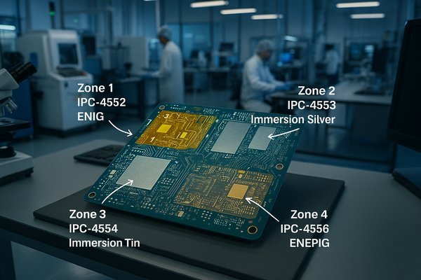
IPC publishes specific standards for common PCB surface finishes, detailing requirements for thickness, appearance, solderability, and testing. Key standards include IPC-4552 (ENIG), IPC-4553 (Immersion Silver), IPC-4554 (Immersion Tin), and IPC-4556 (ENEPIG).
Knowing and referencing these IPC standards is vital for ensuring quality and consistency in PCB manufacturing. When I specify a surface finish on a fabrication drawing, I always call out the relevant IPC standard and class (if applicable). This provides a clear, common understanding between me and the PCB supplier regarding the expected quality and acceptance criteria. It helps avoid misunderstandings and ensures the delivered boards meet the necessary performance and reliability requirements.
Understanding Key IPC Standards for Surface Finishes
IPC standards are developed through industry consensus and provide a valuable framework for manufacturers, designers, and assemblers. For surface finishes, these standards typically cover:
- Scope and Purpose: Defines what the standard covers.
- Applicable Documents: Lists other relevant standards.
- Requirements: Details specific criteria such as:
- Thickness: Specifies minimum, maximum, or typical thickness ranges for each metallic layer. For example, IPC-4552B for ENIG specifies an electroless nickel thickness of \(3 \text{ to } 6 \mu\text{m}\) (\(118.1 \text{ to } 236.2 \mu\text{in}\)) and an immersion gold thickness of \(0.05 \mu\text{m}\) (\(1.97 \mu\text{in}\)) minimum, with a typical maximum around \(0.125 \mu\text{m}\) (\(4.92 \mu\text{in}\)).
- Appearance: Describes visual acceptability criteria (e.g., uniformity, absence of nodules, blisters).
- Purity/Composition: May specify limits for contaminants or alloying elements (e.g., phosphorus content in ENIG's nickel layer, typically \(6-10\%\) per IPC-4552B).
- Solderability: Defines test methods (e.g., wetting balance, dip-and-look) and acceptance criteria for solderability after plating and often after accelerated aging (e.g., steam aging).
- Porosity: For finishes like gold, porosity tests (e.g., nitric acid vapor test) might be specified to ensure the underlying nickel is adequately protected.
- Quality Assurance Provisions: Outlines test methods, sampling plans (e.g., per IPC-A-600 "Acceptability of Printed Boards"), and inspection requirements.
- Preparation for Delivery: May cover packaging and handling to maintain finish integrity.
Here's a brief overview of some key IPC standards for surface finishes:
| Standard Number | Title | Key Aspects Covered | Ni Thick. (\(\mu\text{m}\)) | Finish Thick. (\(\mu\text{m}\)) |
|---|---|---|---|---|
| IPC-4552B | Spec for ENIG (Ni/Au) Plating for PCBs | Ni: \(3-6 \mu\text{m}\), Au: \(0.05-0.125 \mu\text{m}\), P: \(6-10\% \text{ wt.}\); Corrosion, solderability, wire bond. | \(3.0 - 6.0\) | Gold: \(0.05 \mu\text{m} \text{ min }\) \(\text{(often } 0.05-0.125 \mu\text{m})\) |
| IPC-4553A | Spec for ImAg (Imm. Silver) Plating for PCBs | Ag: \(0.12-0.40 \mu\text{m}\); Appearance, solderability, anti-tarnish, packaging. | N/A | Silver: \(0.12 - 0.40 \mu\text{m}\) |
| IPC-4554A | Spec for ImSn (Imm. Tin) Plating for PCBs | Sn: \(1.0 \mu\text{m min, }\) \(\text{target } >1.15 \mu\text{m}\); Solderability, IMC growth, whiskers. | N/A | Tin: \(>1.0 \mu\text{m }\) \(\text{(target } 1.15-1.30 \mu\text{m})\) |
| IPC-4556A | Spec for ENEPIG (Ni/Pd/Au) Plating | Ni: \(3-6 \mu\text{m}\), Pd: \(0.05-0.30 \mu\text{m}\), Au: \(0.03-0.1 \mu\text{m}\); Layers, solderability, wire bond. | \(3.0 - 6.0\) | Pd: \(0.05-0.30 \mu\text{m}\); Au: \(0.03-0.1 \mu\text{m}\) |
| IPC-6012E | Qual. & Perf. Spec for Rigid PCBs | General perf. & qual. reqs for rigid PCBs; Incl. surf. finish integrity. | (References above) | (References above) |
These standards are periodically reviewed and updated by IPC task groups. For instance, IPC-4552 has seen revisions and amendments related to gold thickness and addressing concerns like "black pad." It's always a good idea to ensure you are referencing the latest revision of any IPC standard. Adherence to these standards, especially when coupled with choosing a reputable fabricator certified to IPC-A-600 Class 2 or Class 3 (as appropriate for the product), is a solid step towards achieving reliable and high-quality PCBs.
What Are the Environmental Impacts of Different PCB Surface Finishes?
Concerned about the environmental footprint of your designs? The choice of PCB surface finish involves different chemicals and processes, each with its own environmental considerations.
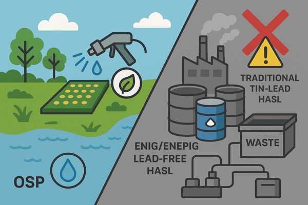
Lead-free HASL (using tin-copper or tin-silver alloys), OSP, and ENIG/ENEPIG are generally RoHS compliant. Traditional tin-lead HASL is not. OSP is often considered more environmentally friendly due to its water-based application and absence of metals in the coating itself, but metal-based finishes require careful waste treatment.
As engineers, we're increasingly aware of the lifecycle impact of our products. The chemicals used in PCB fabrication, including those for surface finishes, can be potent. While RoHS compliance addresses specific hazardous substances, the broader environmental impact of the manufacturing process—water usage, energy consumption, and waste stream management—also matters. I've found that discussing these aspects with PCB fabricators who are transparent about their environmental management systems is becoming more common and important.
The Environmental Side of PCB Finishes: A Detailed View
The environmental impact of PCB surface finishes can be assessed based on several factors:
-
RoHS Compliance: This is a primary driver. Finishes must not contain restricted substances like lead, mercury, cadmium, hexavalent chromium, PBBs, and PBDEs above specified limits (typically \(<0.1\%\) or \(1000 \text{ ppm}\) by weight, cadmium \(<0.01\%\) or \(100 \text{ ppm}\)).
- Compliant: LF HASL, OSP, ImAg, ImSn, ENIG, ENEPIG.
- Non-Compliant: Traditional SnPb HASL (due to lead).
-
Chemicals Used and Waste Generated:
- HASL (SnPb): Uses molten tin-lead solder. Lead is a major environmental and health concern. Dross and sludge containing lead require hazardous waste disposal. Fluxes used can also be aggressive and require treatment.
- LF HASL: Uses tin-copper, tin-silver, or other lead-free alloys (e.g., SN100C: Sn-Cu-Ni-Ge). While lead is eliminated, the high process temperatures (around \(260-270^{\circ}\text{C}\)) consume more energy. Flux chemistry and lead-free dross are still concerns, though less toxic than leaded dross.
- OSP (Organic Solderability Preservatives): Generally considered one of the more environmentally friendly options. These are water-based organic coatings (e.g., azole-based compounds like benzotriazoles or imidazoles). The process involves fewer hazardous chemicals compared to metallic finishes. Waste streams are typically less problematic, mainly consisting of organic residues.
- ImAg (Immersion Silver): Uses silver nitrate and other complexing agents. Silver is a heavy metal, and wastewater treatment is crucial to recover silver (often to \(<0.1 \text{ ppm}\) in effluent, depending on local regulations) and prevent its release. It's RoHS compliant.
- ImSn (Immersion Tin): Uses tin salts (e.g., tin sulfate or tin methane sulfonate). Tin itself is relatively benign, but the plating baths can contain thiourea (a suspected carcinogen) or other strong complexing agents, requiring careful wastewater treatment.
- ENIG (Electroless Nickel Immersion Gold): Involves nickel salts (e.g., nickel sulfate; nickel is a potential carcinogen and skin sensitizer) and gold cyanide or non-cyanide gold complexes. The electroless nickel bath uses reducing agents like sodium hypophosphite and various stabilizers. Wastewater treatment is complex due to the presence of heavy metals (nickel, gold) and complexing agents (e.g., chelators for nickel).
- ENEPIG (Electroless Nickel Electroless Palladium Immersion Gold): Similar to ENIG but with an additional electroless palladium step (using palladium salts). This adds to the chemical complexity and waste treatment requirements for palladium recovery.
-
Energy Consumption:
- HASL processes (both leaded and lead-free) require high temperatures to keep solder molten, leading to higher energy consumption during application.
- Electroless plating processes (ENIG, ENEPIG, ImSn, ImAg) require heated baths, typically in the range of \(40-90^{\circ}\text{C}\) (depending on the specific step), for extended periods.
- OSP application is generally a lower-temperature process, often near room temperature or slightly elevated (e.g., \(40-60^{\circ}\text{C}\)).
-
Water Usage:
- All wet chemical plating processes involve significant water usage for bath make-up, rinsing (multiple stages), and cleaning. Effective water recycling and wastewater treatment systems are essential to minimize consumption and environmental discharge. Fabricators may implement cascade rinsing or other water-saving techniques.
General Comparison of Environmental Friendliness (Lower is Better Score):
| Finish | RoHS Compliant | Chemical Hazard Level | Waste Treatment Complexity | Energy Consumption | Relative "Greenness" Score (1=Best, 5=Worst) |
|---|---|---|---|---|---|
| SnPb HASL | No | High (Lead) | Moderate | High | 5 |
| LF HASL | Yes | Moderate | Moderate | High | 4 |
| OSP | Yes | Low | Low | Low | 1 |
| ImAg | Yes | Moderate (Silver) | Moderate-High | Medium | 3 |
| ImSn | Yes | Moderate (Thiourea) | Moderate | Medium | 3 |
| ENIG | Yes | High (Ni, Au chem) | High | Medium-High | 4 |
| ENEPIG | Yes | High (Ni, Pd, Au chem) | High | Medium-High | 4 |
This table provides a simplified relative comparison. Actual impacts depend heavily on the specific chemistries used by the fabricator and their environmental management practices (e.g., ISO 14001 certification).
Many fabricators are adopting greener chemistries (e.g., cyanide-free gold baths, less hazardous complexing agents) and improving their waste treatment and resource management processes. As an engineer, asking about a supplier's environmental policies, certifications (like ISO 14001), and waste handling procedures can help you choose partners who are more aligned with sustainability goals.
Conclusion
Selecting the right RoHS compliant PCB surface finish involves balancing performance, cost, and environmental factors. Finishes like LF HASL, ENIG, OSP, ImAg, ImSn, and ENEPIG offer compliant solutions for modern electronics.
-
Understanding the skin effect is crucial for optimizing high-speed signal integrity in electrical designs. ↩


