 Skip to content
Struggling with a product that has disappointing wireless range? It's a frustrating problem that can delay projects and cause major headaches. You've followed the design guides, but the performance just isn't there.
The most common reasons for poor PCB antenna range are impedance mismatch, improper ground plane design, interference from nearby components, and the negative effects of the product's enclosure. These factors detune the antenna, preventing it from efficiently radiating power at its target frequency.
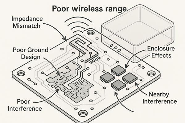
If your device isn't communicating as far as it should, you're in the right place. As a hardware engineer who has designed and debugged wireless systems for everything from security keypads to medical devices, I've spent countless hours troubleshooting these exact issues. I’ve learned that success isn't about secret formulas, but about rigorously applying a few fundamental principles that are easy to overlook. We will explore the critical factors that make or break antenna performance and provide clear, actionable steps to fix them. Let’s dive in.
How Can PCB Antenna Range Be Improved?
Are you trying to squeeze out every last meter of wireless range? It can feel like you're fighting a losing battle when performance still falls short after weeks of work.
To improve range, you must achieve a \(50 \Omega\) impedance match using a VNA, maintain a large clearance area around the antenna, select the right PCB substrate, and account for the enclosure. Optimizing these four areas ensures maximum power transfer from your radio to the air.

Key Steps for Optimizing Antenna Range
Improving antenna performance is a systematic process, not guesswork. It starts with understanding that an antenna is not just a piece of copper trace; it's a complete system that includes the feedline, the matching network, the ground plane, and its surrounding environment.
1. Perfecting the Impedance Match
The industry standard for most RF systems is a characteristic impedance of \(50 \Omega\). This applies not only to the antenna but also to the microstrip or coplanar waveguide trace that connects your radio chip to the matching network and antenna. Use a PCB trace impedance calculator to determine the correct width for this feedline based on your PCB stack-up. A mismatch anywhere in this chain reflects power back to the transmitter instead of radiating it. We measure this reflection using Return Loss1 (\(S_{11}\)).
- Good: A return loss of \(-10 \text{ dB}\) or better is a common target. This means 90% of the power is being delivered to the antenna.
- Excellent: A return loss of \(-15 \text{ dB}\) means over 96% of the power is delivered.
You achieve this match using a Pi-network, a small circuit of capacitors and inductors placed between the radio and the antenna feedline.
2. Substrate and Component Choice
For frequencies \(<1 \text{ GHz}\), standard FR-4 is often acceptable. But for 2.4 GHz (Wi-Fi/BLE) and higher, the material's properties become critical. The table below compares the most common choices.
| Property | Standard FR-4 | High-Frequency (e.g., Rogers RO4350B) | Impact on 2.4 GHz Antenna |
|---|---|---|---|
| Dielectric Constant (\(D_{k}\)) | \(\approx 4.5\) (Varies) | \(\approx 3.48\) (Stable) | Stable \(D_{k}\) ensures consistent resonant frequency. |
| Dissipation Factor (\(D_{f}\)) | \(\approx 0.02\) (High) | \(\approx 0.0037\) (Low) | Lower \(D_{f}\) means less signal loss and higher efficiency. |
| Moisture Absorption | High | Low | FR-4 can detune in humid environments. |
| Relative Cost | Low | High (3x - 10x FR-4) | A key design trade-off. |
While more expensive, a high-frequency laminate is often a necessary investment. For a cost-effective solution, consider a hybrid PCB stack-up that uses Rogers material for the outer RF layers and standard FR-4 for the inner core layers.
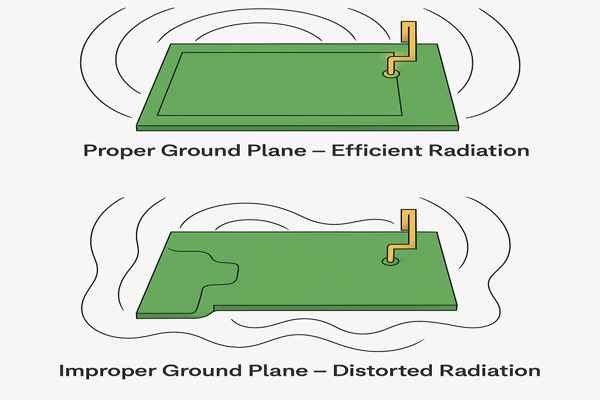
How Does the Ground Plane Affect PCB Antenna Performance?
Did you carefully copy a reference antenna design but it still fails? The ground plane, or lack thereof, might be the invisible culprit sabotaging your performance.
The ground plane is not just a signal return path; it is an active part of the antenna system. For common monopole-type antennas (like Inverted-F antennas), the ground plane acts as the counterpoise. Its size, shape, and clearance directly impact the antenna's impedance and radiation efficiency.
The Ground Plane's Critical Role in Performance
Think of a simple monopole antenna—the ground plane is effectively the other half of the antenna. Without a properly designed ground, the antenna has nothing to "push" against, and its ability to radiate is severely crippled. In contrast, a dipole antenna is a more balanced structure and is less dependent on a large ground plane, but it typically requires more physical space.
1. Ground Plane Size Matters
A larger ground plane generally leads to better efficiency and a more predictable radiation pattern. A common rule is to have a ground plane extending at least a quarter-wavelength (\(\frac{\lambda}{4}\)) from the base of the antenna.
- At 2.45 GHz, the wavelength (\(\lambda\)) in free space is about 12.2 cm.
- A quarter-wavelength (\(\frac{\lambda}{4}\)) is about 3 cm. A ground plane smaller than this will cause the antenna's radiation resistance to drop significantly, making it extremely difficult to match to \(50 \Omega\) and crippling its efficiency.
2. The Critical Keep-Out Area
You must maintain a "keep-out" zone around the antenna. This area must be free of copper and components on all layers.
- Minimum Clearance: Ensure a clearance of at least 5 mm around the antenna element.
- Recommended Clearance: For optimal performance, a clearance of 10 mm to 15 mm is much better. I saw this firsthand on the Honeywell Tuxedo Keypad project, where extending the ground-free zone by just a few millimeters gave us a measurable 2 dB improvement in signal strength.
| Item to Avoid in Keep-Out Zone | Reason |
|---|---|
| Ground/Signal Traces | Detunes the antenna, alters impedance, and blocks radiation |
| Vias | Creates parasitic capacitance/inductance |
| Metal Screws/Hardware | Acts as a parasitic element, reflecting or absorbing RF |
| Batteries & LCDs | Large metal objects that absorb/reflect RF energy |
| Other PCBs | Can couple with the antenna, causing interference |
| Wiring Harnesses | Can act as unintentional antennas, disrupting the pattern |
3. Via Stitching for a Solid Ground
To ensure a low-impedance path for return currents, use dense via stitching to connect ground planes along the entire perimeter of your RF section, not just near the antenna feedpoint. This creates a solid RF ground reference and helps shield sensitive circuits. A common spacing for these vias is between \(\frac{\lambda}{20}\) and \(\frac{\lambda}{10}\) (e.g., about 6 mm to 12 mm apart for 2.4 GHz).
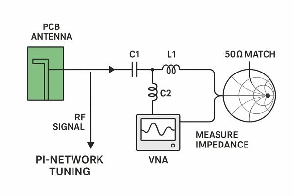
How Are PCB Antennas Tuned?
Your antenna isn't hitting its target frequency, and you know it needs tuning. The process can seem like a dark art, but it's a logical procedure that any engineer can follow.
PCB antennas are tuned using a passive matching network, usually a three-element Pi-network (capacitors and inductors). A Vector Network Analyzer (VNA) is used to measure the antenna's return loss (\(S_{11}\)) and a Smith Chart is used to determine the component values needed to match the antenna's impedance to the system's \(50 \Omega\) impedance at the desired frequency.
The Step-by-Step Tuning Process
Tuning is not an optional step; it's a mandatory part of wireless product development. The goal is to compensate for the real-world effects of your PCB's stack-up, components, and enclosure. When selecting components for your matching network, use high-quality parts. This means using surface-mount inductors with a high \(Q\)-factor and a Self-Resonant Frequency (SRF)2 far above your operating frequency (e.g., \(>6 \text{ GHz}\) for a 2.4 GHz system). For capacitors, use RF-grade, tight-tolerance dielectrics like C0G/NP0 to minimize losses.
| Pi-Network Component | Typical Part | Primary Function in Matching | Smith Chart3 Movement |
|---|---|---|---|
| Shunt Capacitor | High-\(Q\), NP0/C0G | Adds positive susceptance to cancel inductive impedance. | Moves point upwards on a constant conductance circle. |
| Shunt Inductor | High-\(Q\), RF-grade | Adds negative susceptance to cancel capacitive impedance. | Moves point downwards on a constant conductance circle. |
| Series Capacitor | High-\(Q\), NP0/C0G | Adds negative reactance to move along the resistance axis. | Moves counter-clockwise on a constant resistance circle. |
| Series Inductor | High-\(Q\), RF-grade | Adds positive reactance to move along the resistance axis. | Moves clockwise on a constant resistance circle. |
The Tuning Process: A Step-by-Step Guide
- Prepare the Board: Place a Pi-network footprint (e.g., three 0402 pads) between the radio's output and the antenna feedline. Initially, populate the series position with a \(0 \Omega\) resistor and leave the shunt positions empty.
- Connect the VNA: Solder a U.FL connector or semi-rigid coax cable to the input of the matching network. Calibrate your VNA for the frequency band of interest (e.g., 2.4 GHz to 2.5 GHz).
- Measure the Raw Impedance: Measure the \(S_{11}\) of your antenna. The VNA will show a dip on the return loss plot. This is the antenna's current resonant frequency. It will likely be off-target. The VNA will also tell you the impedance at your target frequency (e.g., \(80 - j40 \Omega\)).
- Use a Smith Chart: Plot the measured impedance on a Smith Chart. Your goal is to add components to "move" this point to the center (\(50 \Omega\)). Modern VNA software or standalone tools like SimSmith can automatically calculate the L/C values. For this example, it might suggest a \(1.5 \text{ nH}\) series inductor and a \(0.8 \text{ pF}\) shunt capacitor.
- Place Components and Verify: Solder the calculated component values and measure again. The dip in return loss should now be centered on your target frequency with a value \(<-10 \text{ dB}\). You may need one or two iterations to get it perfect.
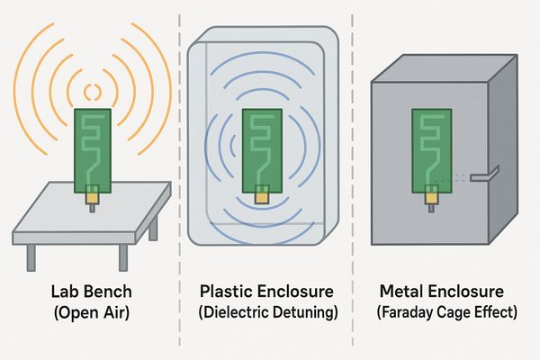
How Do Enclosures Affect PCB Antenna Performance?
Does your board work great on the lab bench, but the range plummets as soon as you put it inside its plastic case? This is a classic problem caused by the enclosure itself.
All enclosures affect antenna performance. Plastic enclosures introduce dielectric loading, which detunes the antenna by lowering its resonant frequency. Metal enclosures act as a Faraday cage, blocking RF signals almost completely unless a specific slot or external antenna is used.
Understanding and Mitigating Enclosure Effects
Failing to account for the product's environment is one of the most common reasons for post-production issues. The final antenna tuning must always be performed with the device fully assembled in its final configuration. The table below summarizes the impact of common materials.
| Material | Dielectric Constant (\(D_{k}\)) | RF Loss | Primary Effect on PCB Antenna | Design Consideration |
|---|---|---|---|---|
| Air (No Enclosure) | \(\approx 1\) | Negligible | Baseline performance. | Ideal for initial testing, but not realistic. |
| ABS Plastic | \(\approx 2.5 - 3.5\) | Low to Moderate | Lowers resonant frequency significantly (dielectric loading). | Must tune antenna inside the final enclosure. |
| Polycarbonate (PC) | \(\approx 2.8 - 3.2\) | Low to Moderate | Similar to ABS; lowers resonant frequency. | Tune in-situ. Verify material consistency from supplier. |
| Aluminum/Steel | N/A (Conductive) | Extremely High (Blocks) | Acts as a Faraday cage, blocking almost all RF signal. | Requires an external antenna or a slot antenna design. |
| Human Hand/Body | High (\(\approx 40-80\)) | Very High (Absorbs) | Drastically detunes antenna and absorbs radiated power. | For wearables, tune with a hand/body phantom. |
Human Body Proximity
For handheld or wearable devices, the effect of the human body is even more severe than plastic. The body is a lossy dielectric that absorbs RF energy and dramatically detunes the antenna. If your product is used in close proximity to a person, you must test and tune it using a "hand phantom" or in its intended real-world use case to ensure it will perform reliably.
Tuning for the Final Assembly
The fix is non-negotiable: perform final antenna tuning with the antenna inside its complete, final enclosure, held as it would be in normal use.
- Assemble the device completely.
- Drill a small hole for the VNA test cable.
- Perform the tuning process. The final component values will be different than those for the bare board.
For metal enclosures, do not place a PCB antenna inside. Use an external antenna or design a slot antenna into the housing itself.
Conclusion
Achieving excellent wireless range is not luck; it's the result of rigorous engineering. By mastering impedance matching, ground plane design, systematic tuning with quality components, and accounting for the final enclosure and user interaction, you can move from frustration to building robust, reliable wireless products.
-
Understanding Return Loss is crucial for optimizing antenna performance and ensuring efficient power delivery. ↩
-
Understanding SRF is crucial for selecting components that minimize losses in RF applications. Explore this link for in-depth insights. ↩
-
The Smith Chart is a powerful tool for visualizing impedance. Learn how to effectively use it for your designs. ↩


