 Skip to content
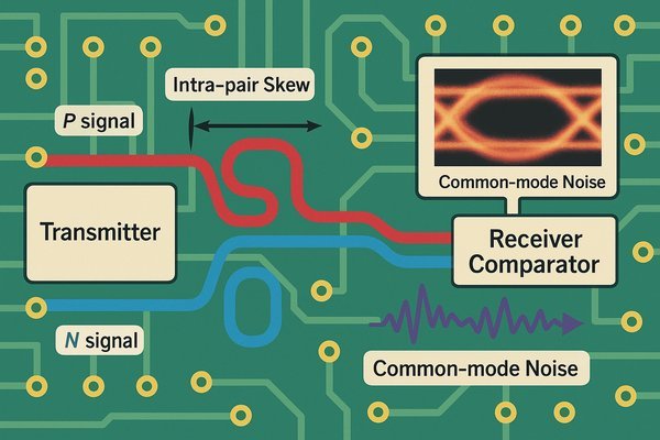
Are your high-speed designs failing intermittently, even when they seem to follow the rules? You might have a subtle timing issue. Mismatched differential pair lengths can introduce skew, a silent killer of signal integrity.
Differential pairs must be length-matched to ensure that the positive (\(P\)) and negative (\(N\)) signals arrive at the receiver's comparator simultaneously. Any length mismatch introduces "intra-pair skew," which collapses the data eye, increases the Bit Error Rate (BER), and converts some of the differential signal into common-mode noise, leading to EMI failures.
I once spent two weeks in the lab chasing a Heisenbug in a new photonic computing evaluation board. The system worked for hours, then would suddenly fall apart with a cascade of data errors. The culprit wasn't firmware or a faulty chip; it was a 20-mil length mismatch in a critical high-speed SERDES link, hidden in the BGA breakout. At \(10+ \text{ Gbps}\), that tiny physical difference was enough to create picoseconds of skew, wrecking the eye diagram under certain conditions. This experience taught me that for serious high-speed design, "close enough" isn't good enough. Precision and foresight are everything.
How Should Differential Pairs Be Laid Out On a PCB?
Struggling to maintain signal integrity across a dense, multi-layer board? The physical layout of your differential pairs is as critical as the silicon you're using. Small deviations can have massive impacts.
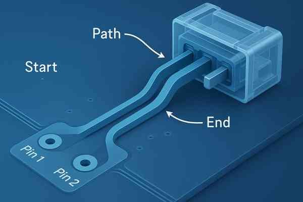
Route differential pairs as a tightly coupled, symmetrical unit. This requires maintaining consistent intra-pair spacing, using a solid reference plane, and mirroring all transitions like bends and vias. Any asymmetry in the routing introduces skew and impedance discontinuities that degrade the signal.
Advanced Layout: Vias, Back-drilling, and Fiber Weave
For an experienced engineer, the basic rules of parallelism and spacing are just the starting point. True high-speed design requires obsessing over the micro-details of the transmission path.
- Minimizing Discontinuities: Every part of the trace path must be managed. This includes not just the main run, but the breakout from the IC package and the entry into the connector. For BGA packages, the fanout routing is critical. I always ensure the escape routes for the \(P\) and \(N\) traces are identical in length and shape. Avoid using a "dog bone" fanout for one trace and a direct route for the other.
- Via Optimization and Back-drilling: Vias are a necessary evil. They introduce significant impedance discontinuities and create stubs. To manage this:
- Always use vias in pairs, placed symmetrically.
- Ensure the anti-pad (the clearance around the via on planes) is correctly sized to minimize capacitance.
- For signals exceeding \(5 \text{ Gbps}\), back-drilling1 is often mandatory. This process removes the unused portion (stub) of the via barrel, which can otherwise cause severe resonant nulls in the frequency response. A 40-mil stub can create a null around \(12-15 \text{ GHz}\), killing your signal.
- Fiber Weave Effect: At speeds above \(10 \text{ Gbps}\), the non-uniform nature of the PCB's fiberglass weave can introduce random, micro-level skew. The dielectric constant of the glass (\(E_{r} \approx 6\)) differs from the epoxy resin (\(E_{r} \approx 3\)). If one trace runs over more glass than its partner, it will travel electrically "slower." To mitigate this, route critical pairs at a slight angle (e.g., 5-10 degrees) to the weave axes, or use materials with a more uniform construction, such as spread-glass weave.
- Routing Topologies: For a single driver and receiver, a point-to-point topology is best. When driving multiple receivers, a "fly-by" topology2 is generally superior to a "star" topology3 as it minimizes disruptive stubs. In a fly-by routing, the trace runs past each receiver, with only a very short tap-off to the IC pads.
Here's a table for advanced considerations:
| Technique | When to Use | Key Parameter / Goal |
|---|---|---|
| Back-Drilling Vias | \(>5 \text{ Gbps}\) | Stub length \(<10 \text{ mils}\). Removes resonant nulls. |
| Angled Routing | \(>10 \text{ Gbps}\) | Route at \(\approx 5^\circ\) to board edge. Averages fiber weave. |
| Optimized Anti-Pad | All high-speed vias | Size to maintain impedance. Prevents excess capacitance. |
| Fly-By Topology | One-to-many links | Minimize stub lengths at each drop. Preserves signal quality. |
Mastering these physical design techniques is what separates a robust, production-ready design from a marginal prototype.
What Is Controlled Impedance for Differential Pairs?
Are you still relying solely on your fab shop's standard stack-up and online calculators? For high-performance designs, you need a deeper understanding of what truly defines impedance and how to control it precisely.
Controlled impedance is the meticulous design of a trace's physical geometry and its relation to reference planes to achieve a target impedance (e.g., \(90\Omega\), \(100\Omega\)). For differential pairs, this impedance (\(Z_{diff}\)) is critical for preventing reflections and ensuring signal integrity. It is not just a number, but a property of the entire transmission path.
Precision Impedance: Field Solvers and Second-Order Effects
Beyond the basic formula, several second-order effects can trip up even experienced engineers. The difference between a \(95\Omega\) and a \(100\Omega\) line can be the margin you need to pass compliance.
- Field Solvers vs. Calculators: Basic online calculators use simplified, closed-form equations. They are great for initial estimates. However, for final verification, a 2D or 2.5D field solver (like those in Cadence Sigrity or Ansys SIwave) is essential. A field solver numerically solves Maxwell's equations for your exact geometry, accounting for effects like trace trapezoid shape and the impact of adjacent traces.
- Impact of Solder Mask: The solder mask is not just a passive coating; it's a dielectric layer. Its presence over a trace will lower the characteristic impedance4, typically by \(2-3\Omega\). A good field solver can model this, but you must know the exact thickness and dielectric constant (\(E_{r}\), usually 3.0-3.5) of the solder mask your fab house uses. For very high-precision designs, I specify "solder mask defined" (SMD) pads or request solder mask be pulled back from critical traces.
- Edge-Coupled vs. Broadside-Coupled: Most designs use edge-coupled pairs, where the traces are side-by-side on the same layer. In extremely dense designs, you can use broadside-coupled pairs, where the traces are routed one on top of the other on adjacent layers. Broadside coupling provides tighter coupling and can save horizontal space but is extremely sensitive to layer-to-layer registration accuracy during manufacturing.
- Process Variation: Your target impedance is a nominal value. The manufacturer will have a process tolerance, typically \(\pm10\%\). For critical applications like RF or precision test equipment, you can specify a \(\pm7\%\) or even \(\pm5\%\) tolerance, but this comes at a significant cost increase. Always ask the fabricator for their standard tolerance and design your system with that margin in mind. I often run simulations at the impedance corners (e.g., \(90\Omega\) and \(110\Omega\) for a \(100\Omega\) nominal line) to ensure my design works across the full manufacturing range.
Here's a comparison of differential pair coupling structures:
| Characteristic | Edge-Coupled | Broadside-Coupled |
|---|---|---|
| Description | Traces are side-by-side on the same PCB layer. | Traces are on top of each other on adjacent layers. |
| Routing Density | Consumes more horizontal space on a layer. | Saves horizontal space, but consumes two layers. |
| Coupling Tightness | Loose to tight, controlled by trace spacing. | Very tight coupling due to thin vertical dielectric. |
| Manufacturing | Less sensitive to manufacturing variations. | Highly sensitive to layer-to-layer registration. |
| Typical Use Case | The vast majority of all differential pair routing. | Extremely dense designs where horizontal space is paramount. |
How Should Differential Pairs Be Routed Through a Connector?
Is your system failing compliance testing at the connector interface? Connectors are a notorious source of impedance discontinuities, and simply picking one with the right datasheet specs isn't enough.
Route differential pairs to adjacent pins in a high-performance connector, maintaining symmetry and minimizing stub length in the breakout region. The goal is to make the transition from PCB to connector pin as electrically invisible as possible by preserving the differential impedance.
The Connector Bottleneck: S-Parameters5 and Breakout Design
The transition from the well-controlled environment of the PCB to the complex 3D structure of a connector is where many high-speed designs fail. A successful transition requires co-design of the PCB layout and connector footprint.
- \(S\)-Parameter Models: For any serious high-speed design (\(>1 \text{ Gbps}\)), don't trust the datasheet alone. Obtain the \(S\)-parameter model for your connector from the manufacturer. This model characterizes the connector's performance across a range of frequencies. You can use this model in a system-level simulation (using ADS, Sigrity, etc.) to see its real-world impact on your signal, including insertion loss6 (\(S_{dd21}\)), return loss (\(S_{dd11}\)), and mode conversion.
- Optimizing the Breakout Region: The area where the traces fan out to meet the connector pads is critical. The tightly-coupled differential traces are forced to separate, causing the impedance to spike. To compensate:
- Keep the uncoupled length as short as humanly possible.
- Strategically place ground vias and cutouts in the reference plane directly under the breakout region. This is called "reference plane stitching" or "ground sculpting" and helps manage the return path and control the impedance of the transition.
- I've often had to reduce the trace width slightly just before the pad to compensate for the pad's capacitance. This requires a field solver to get right.
- Connector Pin Mating Sequence: In hot-pluggable systems (like USB or SATA), the ground pins on the connector are slightly longer, ensuring they mate first and un-mate last. This is crucial for system stability and protecting against ESD. When designing the system, you must account for this behavior.
- Choosing the Right Connector: Don't just pick a "high-speed" connector. Look at its performance data. A connector that is fine for \(5 \text{ Gbps}\) PCIe 3.0 will likely be inadequate for \(10 \text{ Gbps}\) USB 3.1 or \(25 \text{ Gbps}\) Ethernet. Look at the insertion loss at your Nyquist frequency7. A rule of thumb is to keep connector loss under \(1-2 \text{ dB}\) for high-speed channels.
Is a Ground Plane Necessary for Differential Pairs?
Are you tempted to route a differential pair over a split plane to save space? Stop. This is one of the most common and fatal mistakes in high-speed PCB design.
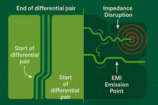
Yes, an unbroken, solid reference plane (usually ground) is absolutely essential. It serves as the primary return path for common-mode currents and is the fundamental reference that defines the pair's characteristic impedance. Routing over a split plane breaks this return path, creating massive impedance discontinuities and radiating EMI.
The Critical Return Path: Mode Conversion and Stitching Vias
The concept of a "zero" return current8 on the ground plane is a theoretical ideal. In practice, every real-world differential pair has some imbalance, creating a common-mode current that must have a low-inductance path back to the source.
- Mode Conversion: When a differential pair crosses a gap in its reference plane, the discontinuity in the return path causes a portion of the differential-mode signal energy to be converted into common-mode energy. This is a phenomenon called mode conversion, which can be measured using \(S\)-parameters (specifically, \(S_{cd21}\) or \(S_{dc21}\)). This newly created common-mode noise is no longer rejected by the receiver and radiates very effectively from the PCB, leading to EMI compliance failures.
- Stitching Vias: If you absolutely must route across different reference planes (e.g., from a ground-referenced layer to a power-referenced layer), you must provide a bridge for the return current. This is done by placing stitching vias9 immediately adjacent to the signal vias. These stitching vias connect the two reference planes and provide a low-inductance path for the return current to follow the signal. I typically use a cluster of 2-4 stitching vias for each critical transition.
- Reference Plane Integrity: The reference plane shouldn't just be present; it must be solid. Avoid placing large numbers of vias in the path of the return current, as this "swiss cheese" effect can raise the plane's impedance. Ensure there is a continuous copper path from the driver's reference to the receiver's reference. On the Tuxedo Keypad, we solved a stubborn EMI issue by adding more stitching vias between our ground planes along the edge of the board, tightening up the entire return path structure.
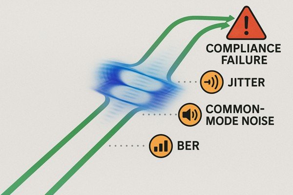
How Does Differential Skew (Intra-Pair Skew) Impact Signal Quality?
Do you know the exact financial cost of skew? A design that fails compliance testing due to skew can mean weeks of delays, costly re-spins, and missed market windows.
Intra-pair skew directly converts differential signal amplitude into common-mode noise and timing jitter. This dual attack shrinks the valid data eye both vertically and horizontally, drastically increasing the bit error rate (BER). The relationship is non-linear; small amounts of skew can have a disproportionately large impact on multi-gigabit signals.
The Picosecond Problem: Quantifying and Measuring Skew
Let's quantify the impact. The amount of differential signal that is converted to common-mode noise is directly proportional to the skew. A simplified formula shows this relationship:
\(V_{CM} \approx \frac{\Delta t}{2 \times t_{rise}} \times V_{DM}\)
Where:
- \(V_{CM}\) is the induced common-mode voltage.
- \(V_{DM}\) is the differential voltage.
- \(\Delta t\) is the intra-pair skew (in picoseconds).
- \(t_{rise}\) is the signal rise time (in picoseconds).
This formula shows that faster rise times make the system far more sensitive to skew. A \(10 \text{ ps}\) skew might be negligible with a \(200 \text{ ps}\) rise time, but it's catastrophic for a signal with a \(30 \text{ ps}\) rise time.
Different standards have strict skew requirements, which dictate the required length matching precision.
| Standard | Data Rate | Max Intra-Pair Skew Allowed | Equivalent Length on FR-4 |
|---|---|---|---|
| USB 2.0 High Speed | \(480 \text{ Mbps}\) | \(100 \text{ ps}\) | \(\approx 15 \text{ mm}\) (600 mils) |
| SATA/PCIe Gen 1 | \(2.5 \text{ GT/s}\) | \(20 \text{ ps}\) | \(\approx 3 \text{ mm}\) (120 mils) |
| USB 3.0 SuperSpeed | \(5.0 \text{ GT/s}\) | \(15 \text{ ps}\) | \(\approx 2.3 \text{ mm}\) (90 mils) |
| PCI Express 3.0 | \(8.0 \text{ GT/s}\) | \(10 \text{ ps}\) | \(\approx 1.5 \text{ mm}\) (60 mils) |
| 10GBASE-KR Ethernet | \(10.3 \text{ Gbps}\) | \(2 \text{ ps}\) | \(\approx 0.3 \text{ mm}\) (12 mils) |
- Measuring Skew: You can't verify picosecond-level matching with a multimeter. Accurate measurement requires a high-bandwidth oscilloscope with Time-Domain Reflectometry10 (TDR) or a Vector Network Analyzer11 (VNA). A TDR sends a fast-edge pulse down the pair and can measure the electrical delay of each line with sub-picosecond resolution. This is a standard step in any serious hardware validation process.
- Sources of Skew: Skew doesn't just come from obvious length mismatches. It can be introduced by asymmetrical routing, via transitions, the fiber weave effect, and IC package skew. Your total skew budget is the sum of all sources: \(\text{Skew}_{\text{Total}} = \text{Skew}_{\text{PCB}} + \text{Skew}_{\text{Package}} + \text{Skew}_{\text{Connector}} + \text{Skew}_{\text{Cable}}\). You must manage the PCB portion with extreme care because it's often the only part you fully control.
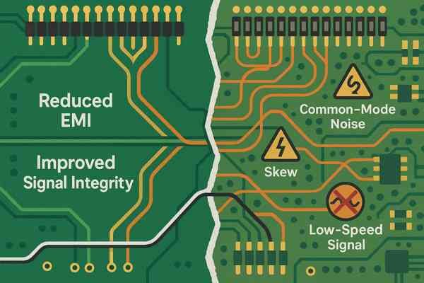
What Are the Limitations of Differential Signaling?
Are you specifying differential pairs for every signal, thinking it's always the superior choice? While incredibly powerful, differential signaling is not a universal solution. It has distinct limitations that can add unnecessary cost and complexity.
Differential signaling's primary drawbacks are its high routing density (doubling trace count and pin count), its susceptibility to common-mode noise exceeding the receiver's input range, and its increased design complexity related to skew and impedance control. It is not always the most efficient solution for lower-speed signals.
Practical Trade-offs: Coupling, Filtering, and Cost
An experienced engineer knows when not to use a specific technology. Here are the practical trade-offs:
- Cost-Benefit Analysis: For low-speed signals (e.g., \(< 50-100 \text{ MHz}\)) in a well-controlled environment, a standard single-ended CMOS signal is often perfectly adequate and much cheaper in terms of board area and routing resources. I've seen junior engineers use LVDS for simple status LEDs, which is massive overkill. The rule is: use the simplest technology that meets the requirements.
- Common-Mode Filtering: While a differential receiver rejects common-mode noise, it doesn't eliminate it. The noise still travels on the lines. In noisy environments, like industrial automation or automotive, you often need to add a common-mode choke (CMC)12 to the differential pair. A CMC is a small magnetic component that presents a high impedance to common-mode currents while allowing differential currents to pass freely. Choosing the right CMC requires analyzing the expected noise spectrum.
- Tight vs. Loose Coupling: There is a design trade-off between tight coupling (traces close together) and loose coupling (traces farther apart).
| Characteristic | Tight Coupling (e.g., \(S=W\)) | Loose Coupling (e.g., \(S=3W\)) |
|---|---|---|
| Noise Immunity | Better rejection of coupled noise (far-field). | More susceptible to external noise due to larger loop area. |
| EMI Performance | Lower radiation due to better field cancellation. | Higher potential for EMI radiation. |
| Routing Ease | Can be more difficult to route in dense areas. | More flexible, easier to route around obstacles. |
| Manufacturing | More sensitive to process variations in spacing. | Less sensitive to manufacturing variations. |
The choice depends on the application. For a noisy industrial environment, I might prioritize the noise rejection of tight coupling. For a very long backplane trace, the robustness of loose coupling might be better.
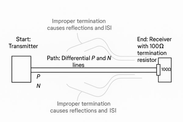
What Is the Proper Way to Terminate Differential Pairs?
Is your termination scheme an afterthought? Improper termination creates reflections that are a primary source of ISI (Inter-Symbol Interference), directly impacting your maximum achievable data rate.
The standard method is to place a single resistor with a value matching the differential impedance (typically \(100\Omega\)) across the \(P\) and \(N\) lines, as close as possible to the receiver's input pins. This absorbs the signal energy and prevents reflections. Many modern ICs include programmable on-chip termination, which should be used when available.
Advanced Termination: ODT, AC Coupling, and Fly-By Topologies
While a single resistor is the most common method, advanced designs require a more nuanced approach.
- On-Chip vs. External Termination: Modern FPGAs and ASICs feature programmable On-Die Termination (ODT)13. ODT is superior to external resistors because it eliminates the stub created by the trace between the resistor and the IC pin, providing a much cleaner termination. It's also programmable, allowing you to adjust the termination scheme via software to optimize signal integrity. If your IC supports ODT, it is almost always the best choice.
- AC vs. DC Coupling: The standard termination scheme is DC-coupled. However, when interfacing between two ICs that have different common-mode voltage requirements, you must use AC coupling14. This involves placing capacitors (typically \(0.1 \mu\text{F}\)) in series on both the \(P\) and \(N\) lines. The termination resistor is then placed on the receiver side of the capacitors. This blocks any DC voltage difference between the driver and receiver. This is the standard for interfaces like SATA, PCIe, and DisplayPort.
- Active Termination: For very high-end applications, you might encounter active termination schemes. These use powered circuits (like op-amps) to provide a more perfect termination across a wider range of conditions than a simple passive resistor can. They are complex and power-hungry, typically reserved for high-performance test equipment or specialized communication links.
- Termination Location in Fly-By Topologies: In a multi-drop fly-by topology, you do not terminate at each receiver. Instead, you place a single termination resistor only at the last device in the chain. Terminating at intermediate devices would create disruptive stubs and improperly load the transmission line.
Here's a summary of common termination strategies:
| Termination Scheme | Description | Primary Advantage | Key Consideration |
|---|---|---|---|
| Standard External | A \(100\Omega\) resistor placed at the receiver. | Simple, effective, and well-understood. | Creates a small trace stub between resistor and IC pin. |
| On-Die (ODT) | Termination is inside the receiver IC. | No stub, best signal integrity. Often programmable. | Only available if the IC supports it. |
| AC-Coupled | Series capacitors before the termination resistor. | Allows ICs with different DC common-mode voltages to connect. | Capacitors must be sized for the data rate. |
Understanding these advanced termination strategies allows you to design robust interfaces that work across different power domains and achieve the highest possible performance.
Conclusion
In high-speed hardware engineering, success lies in mastering the physics of the signal path. Precise control over differential pair length, impedance, routing, and termination isn't just best practice—it's the foundation of a reliable, high-performance product.
-
Learn how back-drilling eliminates via stubs, preventing signal loss and resonant nulls in high-speed PCB designs above 5 Gbps. ↩
-
Learn how fly-by topology improves signal integrity in multi-receiver high-speed circuits and why it's favored over traditional star routing. ↩
-
Learn why 'star' topology can degrade signal quality in high-speed PCB designs and discover better alternatives for robust, production-ready circuits. ↩
-
Gain insights into characteristic impedance to ensure your designs meet electrical performance requirements. ↩
-
Learn how S-parameters help you predict signal integrity issues and optimize high-speed PCB and connector performance in real-world designs. ↩
-
Understanding insertion loss is crucial for ensuring signal integrity in high-speed designs. Learn how it impacts your connector and system performance. ↩
-
Understanding Nyquist frequency is crucial for ensuring signal integrity and minimizing data loss in high-speed electronic designs. ↩
-
Understanding return current is crucial for minimizing EMI and ensuring signal integrity in high-speed PCB designs. Learn best practices from experts. ↩
-
Exploring stitching vias can enhance your PCB designs by providing effective return paths, reducing EMI issues. ↩
-
Explore TDR to learn how it accurately measures skew, essential for validating high-speed signal integrity. ↩
-
Discover the capabilities of a VNA in measuring electrical parameters, vital for precise skew analysis. ↩
-
Discovering the role of common-mode chokes can significantly enhance your understanding of noise management in electronic circuits. ↩
-
Explore the advantages of ODT for signal integrity and programmability in IC designs. ↩
-
Learn about AC coupling's role in managing different common-mode voltages between ICs. ↩


